MEM2302 Specs and Replacement
Type Designator: MEM2302
Type of Transistor: MOSFET
Type of Control Channel: N-Channel
Absolute Maximum Ratings
Pd ⓘ - Maximum Power Dissipation: 1.25 W
|Vds|ⓘ - Maximum Drain-Source Voltage: 20 V
|Vgs|ⓘ - Maximum Gate-Source Voltage: 12 V
|Id| ⓘ - Maximum Drain Current: 5 A
Tj ⓘ - Maximum Junction Temperature: 150 °C
Electrical Characteristics
tr ⓘ - Rise Time: 17 nS
Cossⓘ - Output Capacitance: 105 pF
RDSonⓘ - Maximum Drain-Source On-State Resistance: 0.028 typ Ohm
Package: SOT23
MEM2302 substitution
- MOSFET ⓘ Cross-Reference Search
MEM2302 datasheet
mem2302.pdf
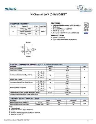
MEM2302 www.VBsemi.tw N-Channel 20 V (D-S) MOSFET FEATURES PRODUCT SUMMARY Halogen-free According to IEC 61249-2-21 VDS (V) RDS(on) ( ) ID (A)e Qg (Typ.) Definition 0.028 at VGS = 4.5 V TrenchFET Power MOSFET 6a 100 % Rg Tested 20 0.042 at VGS = 2.5 V 6a 8.8 nC Compliant to RoHS Directive 2002/95/EC 0.050 at VGS = 1.8 V 5.6 APPLICATIONS DC/DC Conver... See More ⇒
mem2302x.pdf
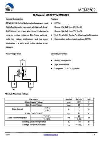
MEM2302 N-Channel MOSFET MEM2302X General Description Features MEM2302XG Series N-channel enhancement mode 20V/3A field-effect transistor ,produced with high cell density RDS(ON) =29m @ VGS=4.5V, ID=3A DMOS trench technology, which is especially used to RDS(ON) =36m @ VGS=2.5V, ID=2A minimize on-state resistance. This device particularly High Density Cell Design For Ultra... See More ⇒
mem2302xg-n.pdf
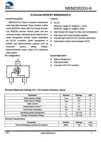
MEM2302XG-N N-Channel MOSFET MEM2302XG-N General Description Features MEM2302XG-N Series N-channel enhancement 20V/3A mode field-effect transistor These miniature surface RDS(ON), Vgs@2.5V, Ids@2.8A = 42m mount MOSFETs utilize High Cell Density process. RDS(ON), Vgs@4.5V, Ids@3A =35m Low RDS(ON) assures minimal power loss and High Density Cell Design For Ultra L... See More ⇒
mem2302m3.pdf
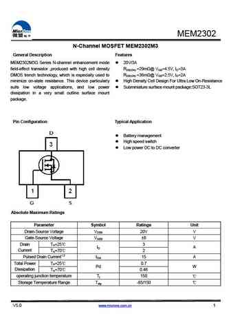
MEM2302 N-Channel MOSFET MEM2302M3 General Description Features MEM2302M3G Series N-channel enhancement mode 20V/3A field-effect transistor ,produced with high cell density RDS(ON) =29m @ VGS=4.5V, ID=3A DMOS trench technology, which is especially used to RDS(ON) =36m @ VGS=2.5V, ID=2A minimize on-state resistance. This device particularly High Density Cell Design For Ultra Low ... See More ⇒
Detailed specifications: LR8103V, LU120N, MDD1653RH, MDU2657RH, MDV1595SU, ME20N10, ME4410, MEM2301, 12N60, MI4800, MMBF0201NLT1G, MMDF3P03HDR, MT2300ACTR, MT4435ACTR, MT4606, MT6680, MTD20N03HDLT4G
Keywords - MEM2302 MOSFET specs
MEM2302 cross reference
MEM2302 equivalent finder
MEM2302 pdf lookup
MEM2302 substitution
MEM2302 replacement
Need a MOSFET replacement? Our guide shows you how to find a perfect substitute by comparing key parameters and specs
🌐 : EN ES РУ

LIST
Last Update
MOSFET: AUB062N08BG | AUB060N08AG | AUB056N10 | AUB056N08BGL | AUB050N085 | AUB050N055 | AUB045N12 | AUB045N10BT | AUB039N10 | AUB034N10
Popular searches
irfb7437 | tip32a | p75nf75 mosfet equivalent | irfpe50 | tip50 | transistor bc547 datasheet | bc109c | d331 transistor