SI2312BDS-T1 Specs and Replacement
Type Designator: SI2312BDS-T1
Type of Transistor: MOSFET
Type of Control Channel: N-Channel
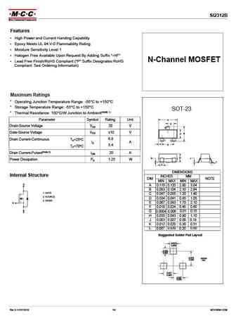
Absolute Maximum Ratings
Pd ⓘ
- Maximum Power Dissipation: 1.25 W
|Vds|ⓘ - Maximum Drain-Source Voltage: 20 V
|Vgs|ⓘ - Maximum Gate-Source Voltage: 12 V
|Id| ⓘ - Maximum Drain Current: 5 A
Tj ⓘ - Maximum Junction Temperature: 150 °C
Electrical Characteristics
tr ⓘ - Rise Time: 17 nS
Cossⓘ -
Output Capacitance: 105 pF
RDSonⓘ - Maximum Drain-Source On-State Resistance: 0.028 typ Ohm
Package: SOT23
SI2312BDS-T1 substitution
- MOSFET ⓘ Cross-Reference Search
SI2312BDS-T1 datasheet
..1. Size:907K cn vbsemi
si2312bds-t1.pdf 
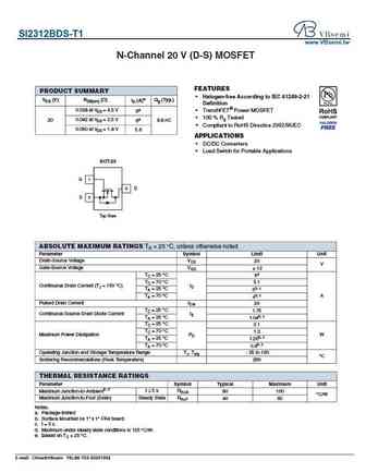
SI2312BDS-T1 www.VBsemi.tw N-Channel 20 V (D-S) MOSFET FEATURES PRODUCT SUMMARY Halogen-free According to IEC 61249-2-21 VDS (V) RDS(on) ( ) ID (A)e Qg (Typ.) Definition 0.028 at VGS = 4.5 V TrenchFET Power MOSFET 6a 100 % Rg Tested 20 0.042 at VGS = 2.5 V 6a 8.8 nC Compliant to RoHS Directive 2002/95/EC 0.050 at VGS = 1.8 V 5.6 APPLICATIONS DC/DC C... See More ⇒
5.1. Size:213K vishay
si2312bds.pdf
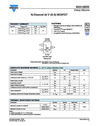
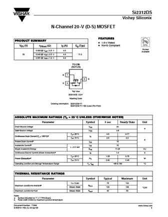
Si2312BDS Vishay Siliconix N-Channel 20 V (D-S) MOSFET FEATURES PRODUCT SUMMARY Halogen-free According to IEC 61249-2-21 VDS (V) RDS(on) ( )ID (A) Qg (Typ.) Definition 0.031 at VGS = 4.5 V 5.0 TrenchFET Power MOSFET 20 0.037 at VGS = 2.5 V 4.6 7.5 100 % Rg Tested 0.047 at VGS = 1.8 V 4.1 Compliant to RoHS Directive 2002/95/EC TO-236 (SOT-23) G 1 3 D S 2... See More ⇒
8.1. Size:126K vishay
si2312cds.pdf
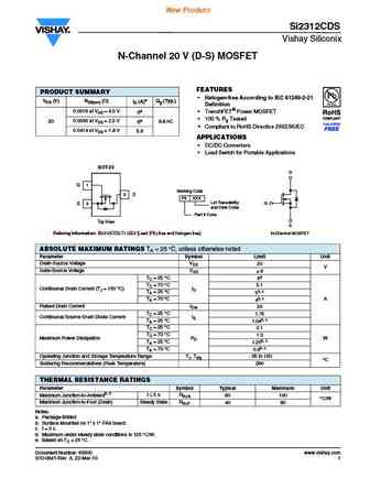
New Product Si2312CDS Vishay Siliconix N-Channel 20 V (D-S) MOSFET FEATURES PRODUCT SUMMARY Halogen-free According to IEC 61249-2-21 VDS (V) RDS(on) ( ) ID (A)e Qg (Typ.) Definition 0.0318 at VGS = 4.5 V TrenchFET Power MOSFET 6a 100 % Rg Tested 20 0.0356 at VGS = 2.5 V 6a 8.8 nC Compliant to RoHS Directive 2002/95/EC 0.0414 at VGS = 1.8 V 5.6 APPLI... See More ⇒
8.2. Size:85K vishay
si2312ds.pdf
Si2312DS Vishay Siliconix N-Channel 20 -V (D-S) MOSFET FEATURES PRODUCT SUMMARY D 1.8-V Rated D RoHS Compliant VDS (V) rDS(on) (W) ID (A) Qg (Typ) Pb-free 0.033 @ VGS = 4.5 V 4.9 Available 0.040 @ VGS = 2.5 V 4.4 20 11.2 0.051 @ VGS = 1.8 V 3.9 TO-236 (SOT-23) G 1 3 D S 2 Top View Si2312DS (C2)* *Marking Code Ordering Information Si2312DS-T1 Si2312DS-T1 E3 (Lead (Pb)-F... See More ⇒
8.3. Size:1882K htsemi
si2312.pdf
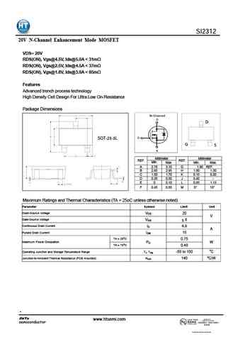
SI2312 20V N-Channel Enhancement Mode MOSFET VDS= 20V RDS(ON), Vgs@4.5V, Ids@5.0A ... See More ⇒
8.4. Size:304K shenzhen
si2312.pdf
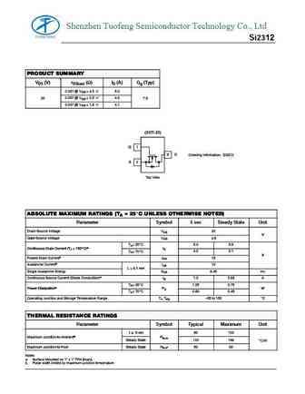
Shenzhen Tuofeng Semiconductor Technology Co., Ltd Si2312 PRODUCT SUMMARY VDS (V) rDS(on) (W) ID (A) Qg (Typ) 0.031 @ VGS = 4.5 V 5.0 0.037 @ VGS = 2.5 V 4.6 20 7.5 0.047 @ VGS = 1.8 V 4.1 (SOT-23) G 1 3 D Ordering Information Si2312 S 2 Top View ABSOLUTE MAXIMUM RATINGS (TA = 25_C UNLESS OTHERWISE NOTED) Parameter Symbol 5 sec Steady State Unit Drain-Source Voltage VDS 20 V ... See More ⇒
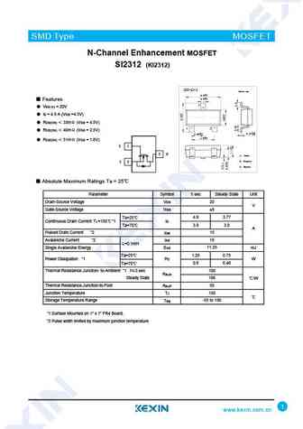
8.5. Size:1696K kexin
si2312ds-3.pdf
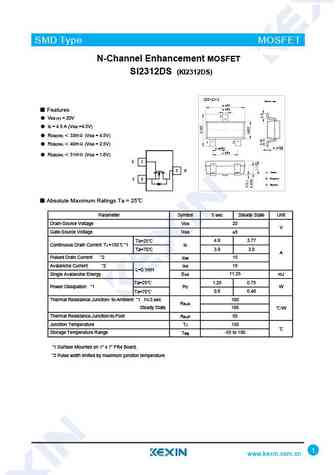
SMD Type MOSFET N-Channel Enhancement MOSFET SI2312DS (KI2312DS) SOT-23-3 Unit mm +0.2 2.9-0.1 +0.1 0.4 -0.1 Features 3 VDS (V) = 20V ID = 4.9 A (VGS =4.5V) RDS(ON) 33m (VGS = 4.5V) 1 2 RDS(ON) 40m (VGS = 2.5V) +0.02 +0.1 0.15 -0.02 0.95 -0.1 +0.1 1.9 -0.2 RDS(ON) 51m (VGS = 1.8V) G 1 3 D 1. Gate 2. Source S 2 3. Drain... See More ⇒
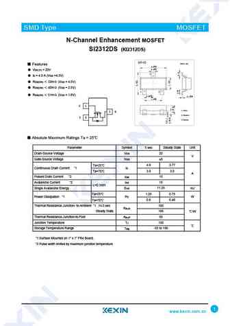
8.6. Size:1794K kexin
si2312 ki2312.pdf
SMD Type MOSFET N-Channel Enhancement MOSFET SI2312 (KI2312) SOT-23-3 Unit mm +0.2 2.9-0.1 +0.1 0.4 -0.1 Features 3 VDS (V) = 20V ID = 4.9 A (VGS =4.5V) RDS(ON) 33m (VGS = 4.5V) 1 2 RDS(ON) 40m (VGS = 2.5V) +0.02 +0.1 0.15 -0.02 0.95 -0.1 +0.1 1.9 -0.2 RDS(ON) 51m (VGS = 1.8V) G 1 3 D 1. Gate 2. Source S 2 3. Drain Abs... See More ⇒
8.7. Size:1660K kexin
si2312ds.pdf
SMD Type MOSFET N-Channel Enhancement MOSFET SI2312DS (KI2312DS) SOT-23 Unit mm Features +0.1 2.9-0.1 +0.1 0.4 -0.1 VDS (V) = 20V 3 ID = 4.9 A (VGS =4.5V) RDS(ON) 33m (VGS = 4.5V) RDS(ON) 40m (VGS = 2.5V) 1 2 RDS(ON) 51m (VGS = 1.8V) +0.1 +0.05 0.95 -0.1 0.1 -0.01 1.9+0.1 -0.1 G 1 1.Gate 3 D 2.Source S 2 3.Drain Abs... See More ⇒
8.8. Size:1799K umw-ic
si2312a.pdf
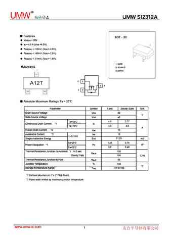
R UMW UMW SI2312A UMW SI2312A Features SOT 23 VDS (V) = 20V ID = 4.9 A (VGS =4.5V) RDS(ON) 33m (VGS = 4.5V) RDS(ON) 40m (VGS = 2.5V) RDS(ON) 51m (VGS = 1.8V) 1. GATE MARKING 2. SOURCE 3. DRAIN G 1 A12T 3 D S 2 Absolute Maximum Ratings Ta = 25 Parameter Symbol 5 sec Steady State Unit Drain-Source Voltage VDS 20 V Gate... See More ⇒
8.9. Size:1164K cn puolop
si2312.pdf
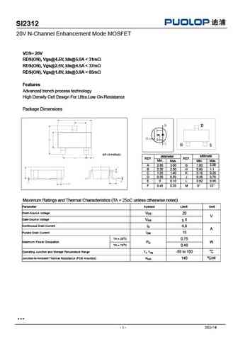
SI2312 20V N-Channel Enhancement Mode MOSFET VDS= 20V RDS(ON), Vgs@4.5V, Ids@5.0A ... See More ⇒
8.10. Size:876K cn vbsemi
si2312cds-t1-ge3.pdf
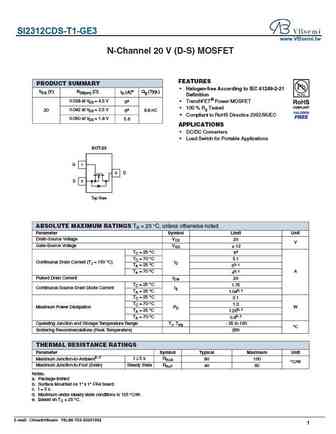
SI2312CDS-T1-GE3 www.VBsemi.tw N-Channel 20 V (D-S) MOSFET FEATURES PRODUCT SUMMARY Halogen-free According to IEC 61249-2-21 VDS (V) RDS(on) ( ) ID (A)e Qg (Typ.) Definition 0.028 at VGS = 4.5 V TrenchFET Power MOSFET 6a 100 % Rg Tested 20 0.042 at VGS = 2.5 V 6a 8.8 nC Compliant to RoHS Directive 2002/95/EC 0.050 at VGS = 1.8 V 5.6 APPLICATIONS DC/... See More ⇒
8.11. Size:1476K cn vbsemi
si2312ds.pdf
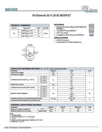
SI2312DS www.VBsemi.tw N-Channel 20 V (D-S) MOSFET FEATURES PRODUCT SUMMARY Halogen-free According to IEC 61249-2-21 VDS (V) RDS(on) ( ) ID (A)e Qg (Typ.) Definition 0.028 at VGS = 4.5 V TrenchFET Power MOSFET 6a 100 % Rg Tested 20 0.042 at VGS = 2.5 V 6a 8.8 nC Compliant to RoHS Directive 2002/95/EC 0.050 at VGS = 1.8 V 5.6 APPLICATIONS DC/DC Conve... See More ⇒
Detailed specifications: SI2301CDS-T1, SI2301DS-T1-GE3, SI2302CDS-T1-GE3, SI2302DS-T1-GE3, SI2305ADS-T1-GE3, SI2305CDS-T1-GE3, SI2305DS-T1-GE3, SI2309CDS-T1-GE3, P55NF06, SI2312CDS-T1-GE3, SI2324DS-T1-GE3, SI2333CDS-T1-GE3, SI2333DDS-T1, SI2333DS-T1-GE3, SI2335DS-T1, SI2342DS-T1, SI2351DS-T1
Keywords - SI2312BDS-T1 MOSFET specs
SI2312BDS-T1 cross reference
SI2312BDS-T1 equivalent finder
SI2312BDS-T1 pdf lookup
SI2312BDS-T1 substitution
SI2312BDS-T1 replacement
Step-by-step guide to finding a MOSFET replacement. Cross-reference parts and ensure compatibility for your repair or project.