ST2300S23RG Specs and Replacement
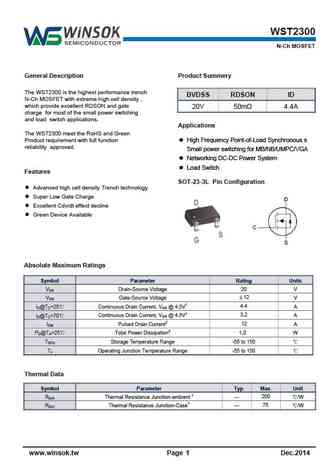
Type Designator: ST2300S23RG
Type of Transistor: MOSFET
Type of Control Channel: N-Channel
Absolute Maximum Ratings
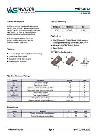
Pd ⓘ - Maximum Power Dissipation: 1.25 W
|Vds|ⓘ - Maximum Drain-Source Voltage: 20 V
|Vgs|ⓘ - Maximum Gate-Source Voltage: 12 V
|Id| ⓘ - Maximum Drain Current: 5 A
Tj ⓘ - Maximum Junction Temperature: 150 °C
Electrical Characteristics
tr ⓘ - Rise Time: 17 nS
Cossⓘ - Output Capacitance: 105 pF
RDSonⓘ - Maximum Drain-Source On-State Resistance: 0.028 typ Ohm
Package: SOT23
ST2300S23RG substitution
- MOSFET ⓘ Cross-Reference Search
ST2300S23RG datasheet
st2300s23rg.pdf
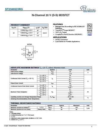
ST2300S23RG www.VBsemi.tw N-Channel 20 V (D-S) MOSFET FEATURES PRODUCT SUMMARY Halogen-free According to IEC 61249-2-21 VDS (V) RDS(on) ( ) ID (A)e Qg (Typ.) Definition 0.028 at VGS = 4.5 V TrenchFET Power MOSFET 6a 100 % Rg Tested 20 0.042 at VGS = 2.5 V 6a 8.8 nC Compliant to RoHS Directive 2002/95/EC 0.050 at VGS = 1.8 V 5.6 APPLICATIONS DC/... See More ⇒
st2300srg.pdf
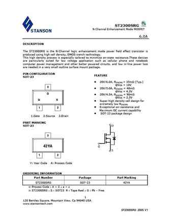
ST2300SRG N Channel Enhancement Mode MOSFET 6.0A DESCRIPTION The ST2300SRG is the N-Channel logic enhancement mode power field effect transistor is produced using high cell density, DMOS trench technology. This high density process is especially tailored to minimize on-state resistance.These devices are particularly suited for low voltage application such as cellular phone and n... See More ⇒
st2300.pdf
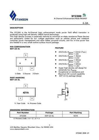
ST2300 N Channel Enhancement Mode MOSFET 6.0A DESCRIPTION The ST2300 is the N-Channel logic enhancement mode power field effect transistor is produced using high cell density, DMOS trench technology. This high density process is especially tailored to minimize on-state resistance.These devices are particularly suited for low voltage application such as cellular phone and noteboo... See More ⇒
jst2300.pdf
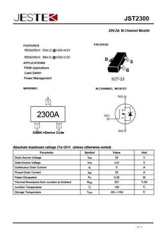
JST2300 20V,5A N-Channel Mosfet PACKAGE FEATURES RDS(ON) 25m @VGS=4.5V RDS(ON) 38m @VGS=2.5V APPLICATIONS PWM Applications Load Switch Power Management MARKING N-CHANNEL MOSFET Absolute maximum ratings (Ta=25 unless otherwise noted) Parameter Symbol Value Unit Drain-Source Voltage V 20 V DS Gate-Source Voltage V 12 V GS Continuous Drain Current I 5 A D Pl... See More ⇒
Detailed specifications: SPN6561S26RGB, SPP3414S23RG, SPP6506S26R, SPP6507S26RGB, SPP80N03S2L, SQ9407EY-T1, SSC8022GS6, SSM2307G, IRF9640, ST2302MSRG, STD10NF06, STD30PF03, STD60NF3L, STD95NH02L, STT8205S, SUD08P06-155, SUD08P06-155L-E3
Keywords - ST2300S23RG MOSFET specs
ST2300S23RG cross reference
ST2300S23RG equivalent finder
ST2300S23RG pdf lookup
ST2300S23RG substitution
ST2300S23RG replacement
Step-by-step guide to finding a MOSFET replacement. Cross-reference parts and ensure compatibility for your repair or project.
🌐 : EN ES РУ
LIST
Last Update
MOSFET: ASD80R750E | ASD70R950E | ASD70R600E | ASD70R380E | ASD65R850E | ASD65R550E | ASD65R350E | ASD65R300E | ASD65R280E | ASD65R270E
Popular searches
d313 transistor equivalent | 2sb827 | c5200 datasheet | 2n2614 | 2sa777 replacement | 2sc828 transistor | 2sd357 | 110n8f6 mosfet datasheet
