VBZE16N05 Specs and Replacement
Type Designator: VBZE16N05
Type of Transistor: MOSFET
Type of Control Channel: N-Channel
Absolute Maximum Ratings
Pd ⓘ - Maximum Power Dissipation: 100 W
|Vds|ⓘ - Maximum Drain-Source Voltage: 60 V
|Vgs|ⓘ - Maximum Gate-Source Voltage: 20 V
|Id| ⓘ - Maximum Drain Current: 41 A
Tj ⓘ - Maximum Junction Temperature: 175 °C
Electrical Characteristics
tr ⓘ - Rise Time: 15 nS
Cossⓘ - Output Capacitance: 140 pF
RDSonⓘ - Maximum Drain-Source On-State Resistance: 0.026 Ohm
Package: TO252
VBZE16N05 substitution
- MOSFET ⓘ Cross-Reference Search
VBZE16N05 datasheet
vbze16n05.pdf
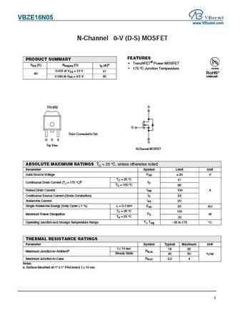
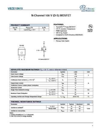
VBZE16N05 www.VBsemi.com N-Channel 6 0-V (D-S) MOSFET FEATURES PRODUCT SUMMARY TrenchFET Power MOSFET VDS (V) RDS(on) ( ) ID (A)a Available 175 C Junction Temperature 0.026 at VGS = 10 V 41 RoHS* 60 0.030 at VGS = 4.5 V 30 COMPLIANT TO-252 D G Drain Connected to Tab G D S S Top View N-Channel MOSFET ABSOLUTE MAXIMUM RATINGS TC = 25 C, unless otherwise noted ... See More ⇒
vbze100n02.pdf
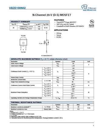
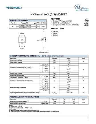
VBZE100N02 www.VBsemi.com N-Channel 20-V (D-S) MOSFET FEATURES PRODUCT SUMMARY TrenchFET Power MOSFET VDS (V) RDS(on) ( ) ID (A)a, e Qg (Typ) 100 % Rg and UIS Tested Compliant to RoHS Directive 2011/65/EU 0.0025 at VGS = 4.5 V 160 20 85 nC 0.006at VGS = 2.5 V 100 APPLICATIONS D OR-ing Server TO-252 DC/DC G G D S Top View S N-Channel MOSFET ... See More ⇒
vbze100p03.pdf
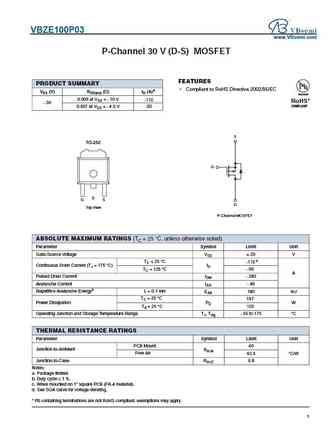
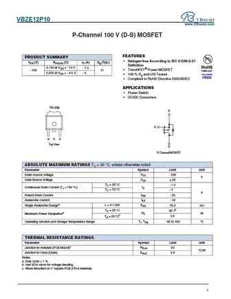
VBZE100P03 www.VBsemi.com P-Channel 30 V (D-S) MOSFET FEATURES PRODUCT SUMMARY Compliant to RoHS Directive 2002/95/EC VDS (V) RDS(on) ( )ID (A)a Available 0.005 at VGS = - 10 V -110 RoHS* - 30 COMPLIANT 0.007 at VGS = - 4.5 V -90 S TO-252 G D G S D Top View P-Channel MOSFET ABSOLUTE MAXIMUM RATINGS (TC = 25 C, unless otherwise noted) Parameter Symbol Limit Unit ... See More ⇒
vbze12n06.pdf
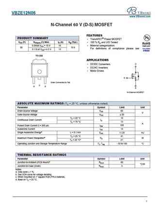
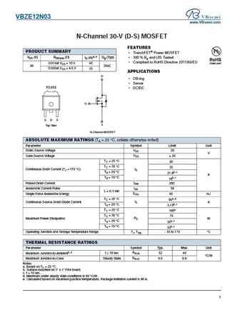
VBZE12N06 www.VBsemi.com N-Channel 60 V (D-S) MOSFET FEATURES PRODUCT SUMMARY TrenchFET Power MOSFET VDS (V) RDS(on) ( ) Max. ID (A) Qg (Typ.) 100 % Rg and UIS Tested 0.095at VGS = 10 V 16 Material categorization 60 19.8 For definitions of compliance please see 0.110 at VGS = 4.5 V 13 TO-252 APPLICATIONS D DC/DC Converters DC/AC Inverters Motor Dr... See More ⇒


Detailed specifications: VBZE100P03, VBZE10N20, VBZE12N03, VBZE12N06, VBZE12N10, VBZE12P10, VBZE15N03, VBZE15N10, RFP50N06, VBZE20N03, VBZE20N06, VBZE20N10, VBZE20N20, VBZE20P03, VBZE20P06, VBZE2810, VBZE2N60
Keywords - VBZE16N05 MOSFET specs
VBZE16N05 cross reference
VBZE16N05 equivalent finder
VBZE16N05 pdf lookup
VBZE16N05 substitution
VBZE16N05 replacement
Need a MOSFET replacement? Our guide shows you how to find a perfect substitute by comparing key parameters and specs
🌐 : EN ES РУ

LIST
Last Update
MOSFET: CM4407 | CM3407 | CM3400 | SVF11N65F | SVF11N65T | FKBB3105 | EHBA036R1 | CRTT067N10N | AP6NA3R2MT | AP65SA145DDT8
Popular searches
2sc1364 | 2sc2320 | d669a transistor | 2sc1419 | 2sc1124 | 2n408 | 2sc2690 | d718 datasheet