VBZE20P06 Specs and Replacement
Type Designator: VBZE20P06
Type of Transistor: MOSFET
Type of Control Channel: P-Channel
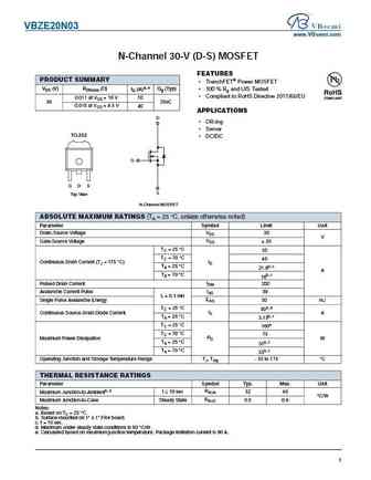
Absolute Maximum Ratings
Pd ⓘ - Maximum Power Dissipation: 34 W
|Vds|ⓘ - Maximum Drain-Source Voltage: 60 V
|Vgs|ⓘ - Maximum Gate-Source Voltage: 20 V
|Id| ⓘ - Maximum Drain Current: 40 A
Tj ⓘ - Maximum Junction Temperature: 175 °C
Electrical Characteristics
tr ⓘ - Rise Time: 15 nS
Cossⓘ - Output Capacitance: 120 pF
RDSonⓘ - Maximum Drain-Source On-State Resistance: 0.061 typ Ohm
Package: TO252
VBZE20P06 substitution
- MOSFET ⓘ Cross-Reference Search
VBZE20P06 datasheet
vbze20p06.pdf
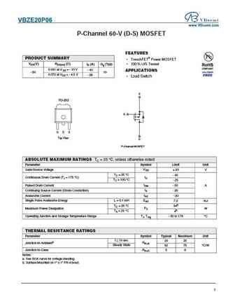
VBZE20P06 www.VBsemi.com P-Channel 60-V (D-S) MOSFET FEATURES PRODUCT SUMMARY TrenchFET Power MOSFET VDS (V) RDS(on) ( ) ID (A) Qg (Typ) 100 % UIS Tested 0.061 at VGS = - 10 V - 40 APPLICATIONS - 60 10 0.072 at VGS = - 4.5 V - 26 Load Switch S TO-252 G G D S Top View D P-Channel MOSFET ABSOLUTE MAXIMUM RATINGS TC = 25 C, unless otherwise noted Parameter Sy... See More ⇒
vbze20p03.pdf
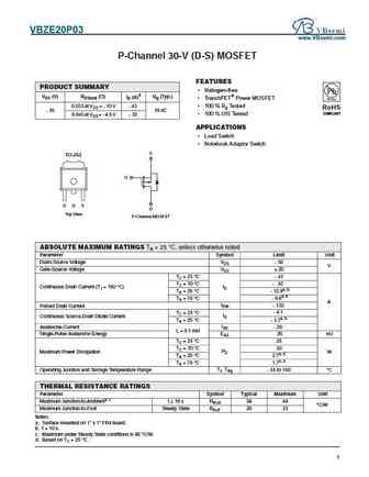
VBZE20P03 www.VBsemi.com P-Channel 30-V (D-S) MOSFET FEATURES PRODUCT SUMMARY Halogen-free VDS (V) RDS(on) ( ) ID (A)d Qg (Typ.) TrenchFET Power MOSFET 0.033 at VGS = - 10 V - 43 100 % Rg Tested RoHS - 30 19 nC COMPLIANT 100 % UIS Tested 0.040 at VGS = - 4.5 V - 30 APPLICATIONS Load Switch Notebook Adaptor Switch S TO-252 G G D S D Top View P-... See More ⇒
vbze20n20.pdf
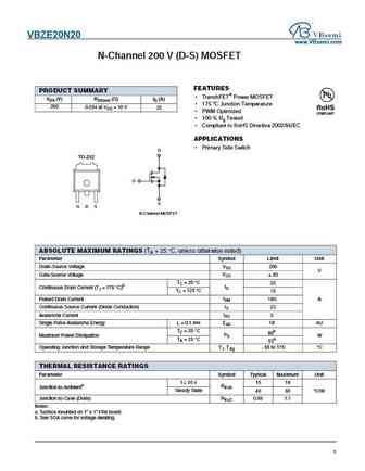
VBZE20N20 www.VBsemi.com N-Channel 200 V (D-S) MOSFET FEATURES PRODUCT SUMMARY TrenchFET Power MOSFET VDS (V) RDS(on) ( )ID (A) 175 C Junction Temperature 200 0.054 at VGS = 10 V 25 PWM Optimized 100 % Rg Tested Compliant to RoHS Directive 2002/95/EC APPLICATIONS Primary Side Switch D TO-252 G S G D S N-Channel MOSFET ABSOLUTE MAXIMUM RATI... See More ⇒
vbze20n10.pdf
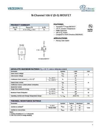
VBZE20N10 www.VBsemi.com N-Channel 100-V (D-S) MOSFET FEATURES PRODUCT SUMMARY TrenchFET Power MOSFET VDS (V) RDS(on) ( )ID (A) 175 C Junction Temperature 100 0.110 at VGS = 10 V 15 PWM Optimized 100 % Rg Tested Compliant to RoHS Directive 2002/95/EC APPLICATIONS Primary Side Switch D TO-252 G S G D S N-Channel MOSFET ABSOLUTE MAXIMUM RATINGS (... See More ⇒
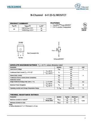
Detailed specifications: VBZE15N03, VBZE15N10, VBZE16N05, VBZE20N03, VBZE20N06, VBZE20N10, VBZE20N20, VBZE20P03, IRF2807, VBZE2810, VBZE2N60, VBZE30N02, VBZE30N03, VBZE30N06, VBZE30N10, VBZE40N03, VBZE40N06
Keywords - VBZE20P06 MOSFET specs
VBZE20P06 cross reference
VBZE20P06 equivalent finder
VBZE20P06 pdf lookup
VBZE20P06 substitution
VBZE20P06 replacement
Step-by-step guide to finding a MOSFET replacement. Cross-reference parts and ensure compatibility for your repair or project.
History: VBZE2810
🌐 : EN ES РУ

LIST
Last Update
MOSFET: CM4407 | CM3407 | CM3400 | SVF11N65F | SVF11N65T | FKBB3105 | EHBA036R1 | CRTT067N10N | AP6NA3R2MT | AP65SA145DDT8
Popular searches
2sc2690 | d718 datasheet | mp38 transistor | 2sc2389 | b331 transistor | 2sa720 | 2sc1345 | 2sd555