FDC6321C Datasheet. Specs and Replacement
Type Designator: FDC6321C 📄📄
Type of Transistor: MOSFET
Type of Control Channel: NP-Channel
Absolute Maximum Ratings
Pd ⓘ - Maximum Power Dissipation: 0.9 W
|Vds|ⓘ - Maximum Drain-Source Voltage: 25 V
|Vgs|ⓘ - Maximum Gate-Source Voltage: 8 V
|Id| ⓘ - Maximum Drain Current: 0.68(0.46) A
Tj ⓘ - Maximum Junction Temperature: 150 °C
Electrical Characteristics
tr ⓘ - Rise Time: 8(9) nS
Cossⓘ - Output Capacitance: 28(34) pF
RDSonⓘ - Maximum Drain-Source On-State Resistance: 0.45(1.1) Ohm
Package: SSOT6
📄📄 Copy
FDC6321C substitution
- MOSFET ⓘ Cross-Reference Search
FDC6321C datasheet
fdc6321c.pdf
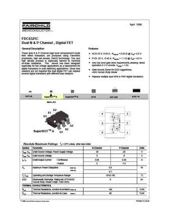
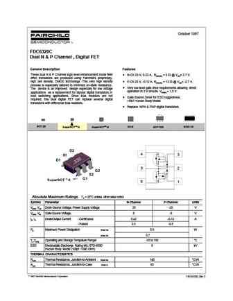
April 1999 FDC6321C Dual N & P Channel , Digital FET General Description Features These dual N & P Channel logic level enhancement mode N-Ch 25 V, 0.68 A, RDS(ON) = 0.45 @ VGS= 4.5 V field effect transistors are produced using Fairchild's proprietary, high cell density, DMOS technology. This very P-Ch -25 V, -0.46 A, RDS(ON) = 1.1 @ VGS= -4.5 V. high density process is especi... See More ⇒
fdc6321c.pdf
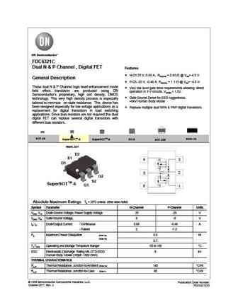
FDC6321C Dual N & P Channel , Digital FET Features N-Ch 25 V, 0.68 A, RDS(ON) = 0.45 @ VGS= 4.5 V General Description P-Ch -25 V, -0.46 A, RDS(ON) = 1.1 @ VGS= -4.5 V. These dual N & P Channel logic level enhancement mode Very low level gate drive requirements allowing direct field effect transistors are produced using ON operation in 3 V circuits. VGS(th) ... See More ⇒
fdc6321c.pdf
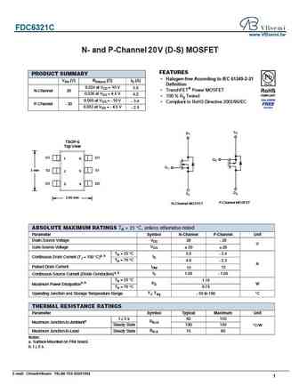
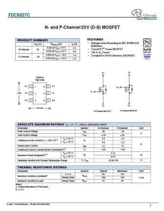
FDC6321C www.VBsemi.tw N- and P-Channel 2 V (D-S) MOSFET 0 FEATURES PRODUCT SUMMARY Halogen-free According to IEC 61249-2-21 VDS (V) RDS(on) ( )ID (A) Definition 0.024 at VGS = 10 V 5.5 TrenchFET Power MOSFET N-Channel 20 0.036 at VGS = 4.5 V 4.2 100 % Rg Tested 0.069 at VGS = - 10 V - 3.4 Compliant to RoHS Directive 2002/95/EC P-Channel - 20 0.083 at V... See More ⇒
fdc6323l.pdf
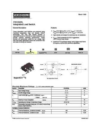
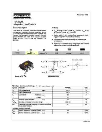
March 1999 FDC6323L Integrated Load Switch General Description Features VDROP=0.2V @ VIN=5V, IL=1A, VON/OFF= 1.5V to 8V These Integrated Load Switches are produced using VDROP=0.3V @ VIN=3.3V, IL=1A, VON/OFF= 1.5V to 8V. Fairchild's proprietary, high cell density, DMOS technology. This very high density process is High density cell design for extremely low on-resistance. especially... See More ⇒

Detailed specifications: FDC606P, FDC608PZ, FDC610PZ, FDC6310P, FDC6312P, FDC6318P, FDC6320C, STU303S, IRF640N, STU3030NLS, FDC6327C, STU17L01, FDC6333C, STU16L01, STU15N20, FDC637BNZ, FDC638APZ
Keywords - FDC6321C MOSFET specs
FDC6321C cross reference
FDC6321C equivalent finder
FDC6321C pdf lookup
FDC6321C substitution
FDC6321C replacement
Learn how to find the right MOSFET substitute. A guide to cross-reference, check specs and replace MOSFETs in your circuits.
MOSFET Parameters. How They Affect Each Other
History: APJ14N65D | VBE1202 | IPI80P03P4L-07 | 2SK4057
🌐 : EN ES РУ

LIST
Last Update
MOSFET: CS95118 | CS85105A | CS75N45 | CS72N12 | CS55N50 | CS48N75A | CS40N27 | MSQ60P04D | MSQ40P07D | MSQ30P40D
Popular searches
tip42c | 2sc2240 | bc547 transistor equivalent | 2sa1943 | tip41c datasheet | mje15032 | tip32c datasheet | mje15032g