VBZMB4N65 Specs and Replacement
Type Designator: VBZMB4N65
Type of Transistor: MOSFET
Type of Control Channel: N-Channel
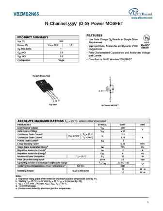
Absolute Maximum Ratings
Pd ⓘ - Maximum Power Dissipation: 30 W
|Vds|ⓘ - Maximum Drain-Source Voltage: 650 V
|Vgs|ⓘ - Maximum Gate-Source Voltage: 30 V
|Id| ⓘ - Maximum Drain Current: 4 A
Tj ⓘ - Maximum Junction Temperature: 150 °C
Electrical Characteristics
tr ⓘ - Rise Time: 20 nS
Cossⓘ - Output Capacitance: 177 pF
RDSonⓘ - Maximum Drain-Source On-State Resistance: 2.5 Ohm
Package: TO220FP
VBZMB4N65 substitution
- MOSFET ⓘ Cross-Reference Search
VBZMB4N65 datasheet
vbzmb4n65.pdf
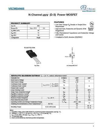
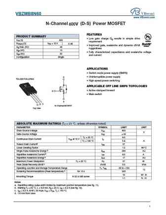
VBZMB4N65 www.VBsemi.com N-Channel (D-S) Power MOSFET 650V FEATURES PRODUCT SUMMARY Low Gate Charge Qg Results in Simple Drive VDS (V) 650 Available Requirement RDS(on) ( )VGS = 10 V 2.5 RoHS* Improved Gate, Avalanche and Dynamic dV/dt COMPLIANT Qg (Max.) (nC) 48 Ruggedness Qgs (nC) 12 Fully Characterized Capacitance and Avalanche Voltage and Current Qgd (nC) 1... See More ⇒
vbzmb12n65.pdf
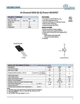
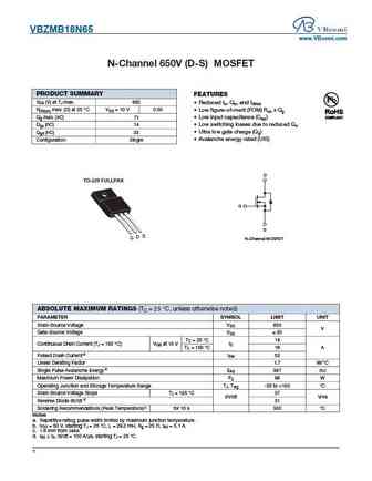
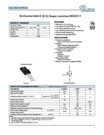
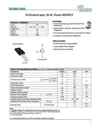
VBZMB12N65 www.VBsemi.com N-Channel 650V (D-S) Power MOSFET FEATURES PRODUCT SUMMARY VDS (V) at TJ max. 650 Low figure-of-merit (FOM) Ron x Qg Low input capacitance (Ciss) RDS(on) max. at 25 C ( ) VGS = 10 V 0.68 43 Reduced switching and conduction losses Qg max. (nC) Ultra low gate charge (Qg) 5 Qgs (nC) Avalanche energy rated (UIS) 22 Qgd (nC) Configu... See More ⇒
vbzmb10n65.pdf
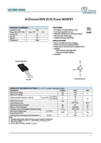
VBZMB10N65 www.VBsemi.com N hannel 650 D S Power MOSFET FEATURES PRODUCT SUMMARY VDS (V) at TJ max. 650 Low figure-of-merit (FOM) Ron x Qg Low input capacitance (Ciss) RDS(on) max. at 25 C ( ) VGS = 10 V 0.9 Reduced switching and conduction losses Qg max. (nC) 57 Ultra low gate charge (Qg) Qgs (nC) 4.0 Avalanche energy rated (UIS) Qgd (nC) 5.4 Config... See More ⇒
vbzmb18n50.pdf
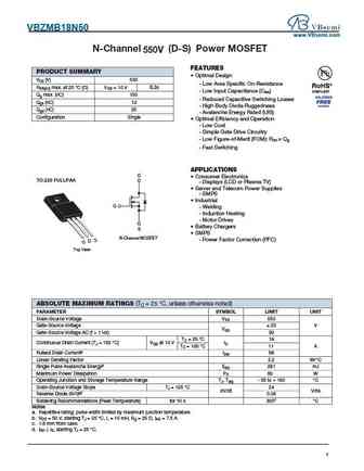
VBZMB18N50 www.VBsemi.com N-Channel (D-S) Power MOSFET 550V FEATURES PRODUCT SUMMARY Optimal Design VDS (V) 550 - Low Area Specific On-Resistance RDS(on) max. at 25 C ( ) VGS = 10 V 0.26 - Low Input Capacitance (Ciss) Qg max. (nC) 150 - Reduced Capacitive Switching Losses Qgs (nC) 12 - High Body Diode Ruggedness Qgd (nC) 25 - Avalanche Energy Rated (UIS) Configuration ... See More ⇒
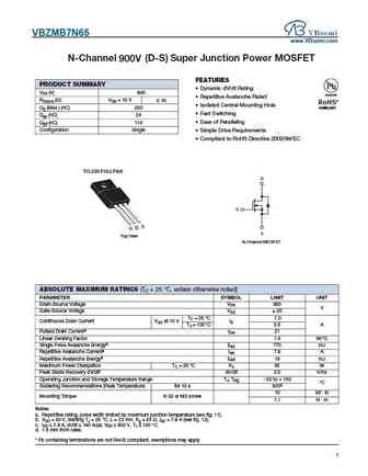
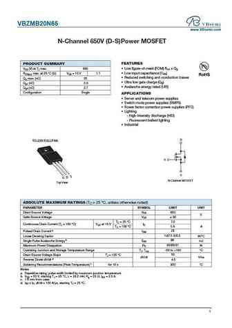
Detailed specifications: VBZMB10N65, VBZMB12N65, VBZMB13N50, VBZMB18N50, VBZMB18N65, VBZMB20N65, VBZMB20N65S, VBZMB2N65, 75N75, VBZMB7N65, VBZMB8N60, VBZP50N50S, VBZQA120N03, VBZQA50N03, VBZQA50P03, VBZQA80N03, VBZQF50N03
Keywords - VBZMB4N65 MOSFET specs
VBZMB4N65 cross reference
VBZMB4N65 equivalent finder
VBZMB4N65 pdf lookup
VBZMB4N65 substitution
VBZMB4N65 replacement
Need a MOSFET replacement? Our guide shows you how to find a perfect substitute by comparing key parameters and specs
🌐 : EN ES РУ

LIST
Last Update
MOSFET: CM4407 | CM3407 | CM3400 | SVF11N65F | SVF11N65T | FKBB3105 | EHBA036R1 | CRTT067N10N | AP6NA3R2MT | AP65SA145DDT8
Popular searches
a1941 datasheet | hrf3205 | c2837 datasheet | 2n414 | c3998 | c4468 datasheet | 2sc2603 | jcs50n20wt