NCE2301 Specs and Replacement
Type Designator: NCE2301
Type of Transistor: MOSFET
Type of Control Channel: P-Channel
Absolute Maximum Ratings
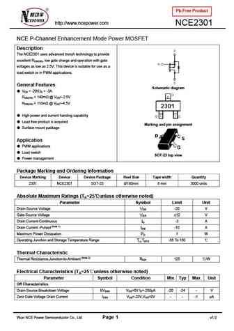
Pd ⓘ - Maximum Power Dissipation: 1 W
|Vds|ⓘ - Maximum Drain-Source Voltage: 20 V
|Vgs|ⓘ - Maximum Gate-Source Voltage: 12 V
|Id| ⓘ - Maximum Drain Current: 3 A
Tj ⓘ - Maximum Junction Temperature: 150 °C
Electrical Characteristics
tr ⓘ - Rise Time: 35 nS
Cossⓘ - Output Capacitance: 75 pF
RDSonⓘ - Maximum Drain-Source On-State Resistance: 0.11 Ohm
Package: SOT23
NCE2301 substitution
- MOSFET ⓘ Cross-Reference Search
NCE2301 datasheet
nce2301.pdf
Pb Free Product http //www.ncepower.com NCE2301 NCE P-Channel Enhancement Mode Power MOSFET Description The NCE2301 uses advanced trench technology to provide excellent RDS(ON), low gate charge and operation with gate voltages as low as 2.5V. This device is suitable for use as a load switch or in PWM applications. General Features Schematic diagram VDS = -20V,ID = -3A ... See More ⇒
nce2301a.pdf
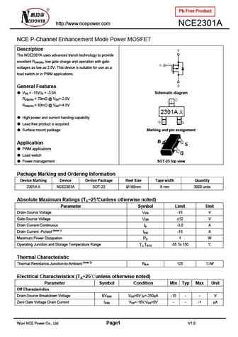
Pb Free Product http //www.ncepower.com NCE2301A NCE P-Channel Enhancement Mode Power MOSFET Description The NCE2301A uses advanced trench technology to provide excellent RDS(ON), low gate charge and operation with gate voltages as low as 2.5V. This device is suitable for use as a load switch or in PWM applications. General Features VDS = -15V,ID = -3.0A Schematic diagram ... See More ⇒
nce2301c.pdf
Pb Free Product http //www.ncepower.com NCE2301C NCE P-Channel Enhancement Mode Power MOSFET Description D The NCE2301C uses advanced trench technology to provide excellent RDS(ON), low gate charge and operation with gate G voltages as low as 1.8V. This device is suitable for use as a load switch or in PWM applications. S General Features Schematic diagram VDS = -15V,... See More ⇒
nce2301e.pdf
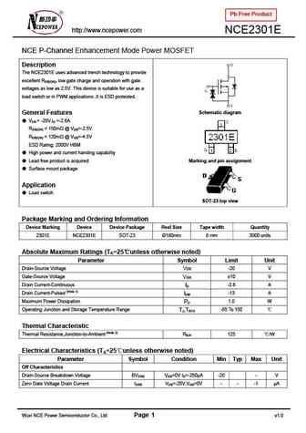
Pb Free Product http //www.ncepower.com NCE2301E NCE P-Channel Enhancement Mode Power MOSFET Description The NCE2301E uses advanced trench technology to provide excellent RDS(ON), low gate charge and operation with gate voltages as low as 2.5V. This device is suitable for use as a load switch or in PWM applications .It is ESD protested. Schematic diagram General Features ... See More ⇒
Detailed specifications: NCE2003, NCE2007N, NCE2010E, NCE2030, NCE2030K, NCE2060K, NCE20P45Q, NCE20P70G, AON7506, NCE2302, NCE2303, NCE2304, NCE2305, NCE2309, NCE2312, NCE2312A, NCE2333Y
Keywords - NCE2301 MOSFET specs
NCE2301 cross reference
NCE2301 equivalent finder
NCE2301 pdf lookup
NCE2301 substitution
NCE2301 replacement
Need a MOSFET replacement? Our guide shows you how to find a perfect substitute by comparing key parameters and specs
🌐 : EN ES РУ
LIST
Last Update
MOSFET: AKF30N5P0SX | AKF30N10S | AKF20P45D | CM4407 | CM3407 | CM3400 | SVF11N65F | SVF11N65T | FKBB3105 | EHBA036R1
Popular searches
tip29 transistor equivalent | 2n555 | 2sa564a | c815 transistor | ksa1381 equivalent | 2sa1306 | b817 transistor | 2n3394


