FDD6685 Specs and Replacement
Type Designator: FDD6685
Type of Transistor: MOSFET
Type of Control Channel: P-Channel
Absolute Maximum Ratings
Pd ⓘ
- Maximum Power Dissipation: 52 W
|Vds|ⓘ - Maximum Drain-Source Voltage: 30 V
|Vgs|ⓘ - Maximum Gate-Source Voltage: 25 V
|Id| ⓘ - Maximum Drain Current: 40 A
Tj ⓘ - Maximum Junction Temperature: 175 °C
Electrical Characteristics
RDSonⓘ - Maximum Drain-Source On-State Resistance: 0.02 Ohm
Package: TO252
DPAK
- MOSFET ⓘ Cross-Reference Search
FDD6685 datasheet
..1. Size:181K fairchild semi
fdd6685.pdf 
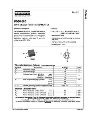
May 2011 FDD6685 30V P-Channel PowerTrench MOSFET General Description Features This P-Channel MOSFET is a rugged gate version of 40 A, 30 V. RDS(ON) = 20 m @ VGS = 10 V RDS(ON) = 30 m @ VGS = 4.5 V Fairchild Semiconductor s advanced PowerTrench Fast switching speed process. It has been optimized for power management applications requiring a wide... See More ⇒
..2. Size:117K onsemi
fdd6685.pdf

February 2004 FDD6685 30V P-Channel PowerTrench MOSFET General Description Features This P-Channel MOSFET is a rugged gate version of 40 A, 30 V. RDS(ON) = 20 m @ VGS = 10 V RDS(ON) = 30 m @ VGS = 4.5 V Fairchild Semiconductor s advanced PowerTrench Fast switching speed process. It has been optimized for power management applications requiring a... See More ⇒
..3. Size:784K cn vbsemi
fdd6685.pdf
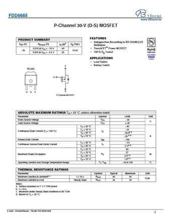
FDD6685 www.VBsemi.tw P-Channel 30-V (D-S) MOSFET FEATURES PRODUCT SUMMARY Halogen-free According to IEC 61249-2-21 VDS (V) RDS(on) ( ) ID (A)d Qg (Typ.) Definition 0.018 at VGS = - 10 V - 40 TrenchFET Power MOSFET - 30 13 nC 100 % Rg Tested 0.025 at VGS = - 4.5 V - 35 APPLICATIONS Load Switch Battery Switch S TO-252 G D G D S P-Channel MOSFET ABS... See More ⇒
8.1. Size:199K fairchild semi
fdd6680.pdf
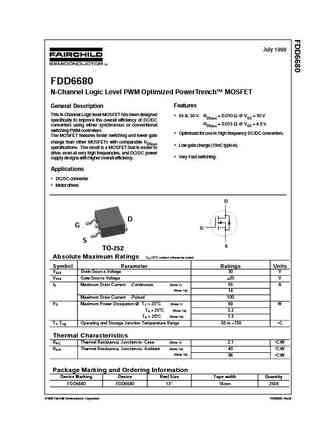
July 1999 FDD6680 N-Channel Logic Level PWM Optimized PowerTrench MOSFET Features General Description This N-Channel Logic level MOSFET has been designed 55 A, 30 V. RDS(on) = 0.010 @ VGS = 10 V specifically to improve the overall efficiency of DC/DC RDS(on) = 0.015 @ VGS = 4.5 V. converters using either synchronous or conventional switching PWM controllers. Optimi... See More ⇒
8.2. Size:327K fairchild semi
fdd6680as.pdf
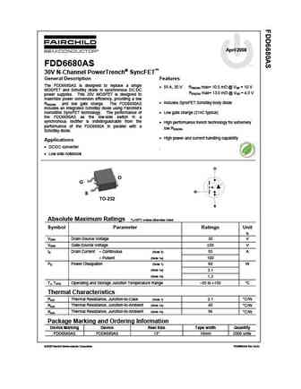
April 2008 FDD6680AS tm 30V N-Channel PowerTrench SyncFET General Description Features The FDD6680AS is designed to replace a single 55 A, 30 V RDS(ON) max= 10.5 m @ VGS = 10 V MOSFET and Schottky diode in synchronous DC DC RDS(ON) max= 13.0 m @ VGS = 4.5 V power supplies. This 30V MOSFET is designed to maximize power conversion efficiency, providing a low ... See More ⇒
8.3. Size:93K fairchild semi
fdd6680s.pdf
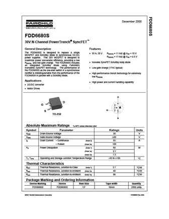
December 2000 FDD6680S 30V N-Channel PowerTrench SyncFET General Description Features The FDD6680S is designed to replace a single 55 A, 30 V RDS(ON) = 11 m @ VGS = 10 V MOSFET and Schottky diode in synchronous DC DC RDS(ON) = 17 m @ VGS = 4.5 V power supplies. This 30V MOSFET is designed to maximize power conversion efficiency, providing a low Inclu... See More ⇒
8.4. Size:121K fairchild semi
fdd6682 dss20201l.pdf

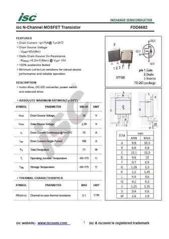
June 2004 FDD6682/FDU6682 30V N-Channel PowerTrench MOSFET General Description Features This N-Channel MOSFET has been designed 75 A, 30 V RDS(ON) = 6.2 m @ VGS = 10 V specifically to improve the overall efficiency of DC/DC RDS(ON) = 8.0 m @ VGS = 4.5 V converters using either synchronous or conventional switching PWM controllers. It has been optimized for Low gate charg... See More ⇒
8.5. Size:688K fairchild semi
fdd6688s.pdf
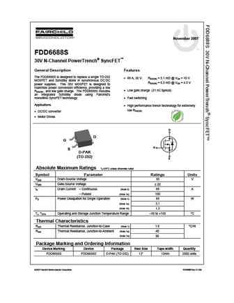
November 2007 tm FDD6688S 30V N-Channel PowerTrench SyncFET General Description Features The FDD6688S is designed to replace a single TO-252 88 A, 30 V. RDS(ON) = 5.1 m @ VGS = 10 V MOSFET and Schottky diode in synchronous DC DC RDS(ON) = 6.3 m @ VGS = 4.5 V power supplies. This 30V MOSFET is designed to maximize power conversion efficiency, providing a low ... See More ⇒
8.6. Size:117K fairchild semi
fdd6682.pdf

June 2004 FDD6682/FDU6682 30V N-Channel PowerTrench MOSFET General Description Features This N-Channel MOSFET has been designed 75 A, 30 V RDS(ON) = 6.2 m @ VGS = 10 V specifically to improve the overall efficiency of DC/DC RDS(ON) = 8.0 m @ VGS = 4.5 V converters using either synchronous or conventional switching PWM controllers. It has been optimized for Low gate charg... See More ⇒
8.7. Size:120K fairchild semi
fdd6688 fdd6688 fdu6688.pdf
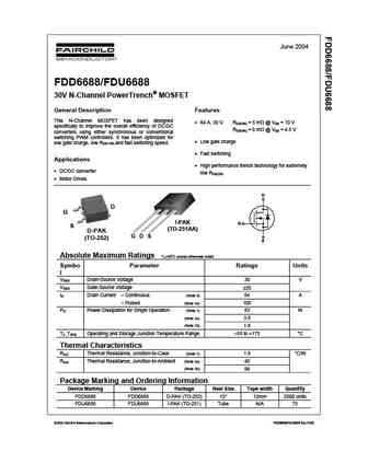
June 2004 FDD6688/FDU6688 30V N-Channel PowerTrench MOSFET General Description Features This N-Channel MOSFET has been designed 84 A, 30 V. RDS(ON) = 5 m @ VGS = 10 V specifically to improve the overall efficiency of DC/DC RDS(ON) = 6 m @ VGS = 4.5 V converters using either synchronous or conventional switching PWM controllers. It has been optimized for Low gate charge ... See More ⇒
8.8. Size:200K fairchild semi
fdd6680a.pdf
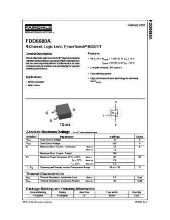
February 2000 FDD6680A N-Channel, Logic Level, PowerTrench MOSFET Features General Description This N-Channel Logic level MOSFET is produced using 56 A, 30 V. RDS(ON) = 0.0095 @ VGS = 10 V Fairchild Semiconductor's advanced PowerTrench process RDS(ON) = 0.0130 @ VGS = 4.5 V. that has been especially tailored to minimize the on-state resistance and y... See More ⇒
8.9. Size:1488K cn vbsemi
fdd6680.pdf
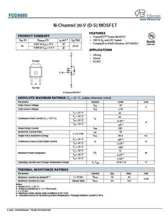
FDD6680 www.VBsemi.tw N-Channel 30-V (D-S) MOSFET FEATURES PRODUCT SUMMARY TrenchFET Power MOSFET VDS (V) RDS(on) ( ) ID (A)a, e Qg (Typ) 100 % Rg and UIS Tested Compliant to RoHS Directive 2011/65/EU 0.007 at VGS = 10 V 50 30 25 nC 0.009 at VGS = 4.5 V 40 APPLICATIONS D OR-ing Server TO-252 DC/DC G G D S S Top View N-Channel MOSFET ABSOLU... See More ⇒
8.10. Size:287K inchange semiconductor
fdd6680.pdf

isc N-Channel MOSFET Transistor FDD6680 FEATURES Drain Current I =46A@ T =25 D C Drain Source Voltage V =30V(Min) DSS Static Drain-Source On-Resistance R =10m (Max) @ V = 10V DS(on) GS 100% avalanche tested Minimum Lot-to-Lot variations for robust device performance and reliable operation DESCRIPTION motor drive, DC-DC converter, power switch and solenoid dr... See More ⇒
8.11. Size:287K inchange semiconductor
fdd6680as.pdf
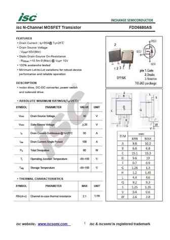
isc N-Channel MOSFET Transistor FDD6680AS FEATURES Drain Current I =55A@ T =25 D C Drain Source Voltage V =30V(Min) DSS Static Drain-Source On-Resistance R =10.5m (Max) @ V = 10V DS(on) GS 100% avalanche tested Minimum Lot-to-Lot variations for robust device performance and reliable operation DESCRIPTION motor drive, DC-DC converter, power switch and solenoi... See More ⇒
8.12. Size:287K inchange semiconductor
fdd6680s.pdf

isc N-Channel MOSFET Transistor FDD6680S FEATURES Drain Current I =55A@ T =25 D C Drain Source Voltage V =30V(Min) DSS Static Drain-Source On-Resistance R =11m (Max) @ V = 10V DS(on) GS 100% avalanche tested Minimum Lot-to-Lot variations for robust device performance and reliable operation DESCRIPTION motor drive, DC-DC converter, power switch and solenoid d... See More ⇒
8.13. Size:287K inchange semiconductor
fdd6688.pdf

isc N-Channel MOSFET Transistor FDD6688 FEATURES Drain Current I =84A@ T =25 D C Drain Source Voltage V =30V(Min) DSS Static Drain-Source On-Resistance R =5m (Max) @ V = 10V DS(on) GS 100% avalanche tested Minimum Lot-to-Lot variations for robust device performance and reliable operation DESCRIPTION motor drive, DC-DC converter, power switch and solenoid dri... See More ⇒
8.14. Size:288K inchange semiconductor
fdd6688s.pdf

isc N-Channel MOSFET Transistor FDD6688S FEATURES Drain Current I =88A@ T =25 D C Drain Source Voltage V =30V(Min) DSS Static Drain-Source On-Resistance R =5.1m (Max) @ V = 10V DS(on) GS 100% avalanche tested Minimum Lot-to-Lot variations for robust device performance and reliable operation DESCRIPTION motor drive, DC-DC converter, power switch and solenoid ... See More ⇒
8.15. Size:287K inchange semiconductor
fdd6682.pdf
isc N-Channel MOSFET Transistor FDD6682 FEATURES Drain Current I =75A@ T =25 D C Drain Source Voltage V =30V(Min) DSS Static Drain-Source On-Resistance R =6.2m (Max) @ V = 10V DS(on) GS 100% avalanche tested Minimum Lot-to-Lot variations for robust device performance and reliable operation DESCRIPTION motor drive, DC-DC converter, power switch and solenoid d... See More ⇒
8.16. Size:287K inchange semiconductor
fdd6680a.pdf

isc N-Channel MOSFET Transistor FDD6680A FEATURES Drain Current I =56A@ T =25 D C Drain Source Voltage V =30V(Min) DSS Static Drain-Source On-Resistance R =9.5m (Max) @ V = 10V DS(on) GS 100% avalanche tested Minimum Lot-to-Lot variations for robust device performance and reliable operation DESCRIPTION motor drive, DC-DC converter, power switch and solenoid ... See More ⇒
Detailed specifications: FDD6530A
, FDD6630A
, STT03N20
, FDD6635
, FDD6637
, FDD6637F085
, FDD6680AS
, STT03N10
, IRFP460
, FDD6760A
, FDD6770A
, FDD6778A
, FDD6780A
, FDD6796A
, FDD6N20TM
, STT03L06
, FDD6N25
.
Keywords - FDD6685 MOSFET specs
FDD6685 cross reference
FDD6685 equivalent finder
FDD6685 pdf lookup
FDD6685 substitution
FDD6685 replacement
Learn how to find the right MOSFET substitute. A guide to cross-reference, check specs and replace MOSFETs in your circuits.
