13N50L-TF3-T Specs and Replacement
Type Designator: 13N50L-TF3-T
Type of Transistor: MOSFET
Type of Control Channel: N-Channel
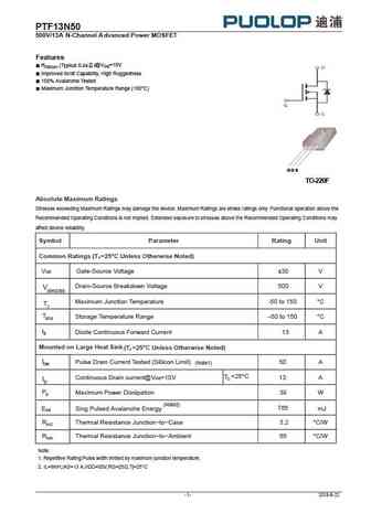
Absolute Maximum Ratings
Pd ⓘ - Maximum Power Dissipation: 35 W
|Vds|ⓘ - Maximum Drain-Source Voltage: 500 V
|Vgs|ⓘ - Maximum Gate-Source Voltage: 30 V
|Id| ⓘ - Maximum Drain Current: 13 A
Tj ⓘ - Maximum Junction Temperature: 150 °C
Electrical Characteristics
tr ⓘ - Rise Time: 158 nS
Cossⓘ - Output Capacitance: 202 pF
RDSonⓘ - Maximum Drain-Source On-State Resistance: 0.48 Ohm
Package: TO-220F
13N50L-TF3-T substitution
- MOSFET ⓘ Cross-Reference Search
13N50L-TF3-T datasheet
13n50l-ta3-t 13n50g-ta3-t 13n50l-tf3-t 13n50g-tf3-t 13n50l-tf1-t 13n50g-tf1-t.pdf
UNISONIC TECHNOLOGIES CO., LTD 13N50 Power MOSFET 13A, 500V N-CHANNEL POWER MOSFET DESCRIPTION The UTC 13N50 is a N-Channel enhancement mode power MOSFET. The device adopts planar stripe and uses DMOS technology to minimize and provide lower on-state resistance and faster switching speed. It can also withstand high energy pulse under the avalanche and commutation mode cond... See More ⇒
13n50l-t2q-t 13n50g-t2q-t 13n50l-tq2-t 13n50g-tq2-t 13n50l-tq2-r 13n50g-tq2-r.pdf

UNISONIC TECHNOLOGIES CO., LTD 13N50 Power MOSFET 13A, 500V N-CHANNEL POWER MOSFET DESCRIPTION The UTC 13N50 is a N-Channel enhancement mode power MOSFET. The device adopts planar stripe and uses DMOS technology to minimize and provide lower on-state resistance and faster switching speed. It can also withstand high energy pulse under the avalanche and commutation mode cond... See More ⇒
jcs13n50ft.pdf
N N- CHANNEL MOSFET R JCS13N50FT MAIN CHARACTERISTICS Package ID 13 A VDSS 500 V Rdson-max @Vgs=10V 0.46 Qg-typ 37 nC APPLICATIONS High frequency switching mode power supply UPS Electronic ballast UPS FEATUR... See More ⇒
irfb13n50apbf.pdf
PD - 95122 SMPS MOSFET IRFB13N50APbF HEXFET Power MOSFET AppIications VDSS RDS(on) max ID l Switch Mode Power Supply (SMPS) l Uninterruptible Power Supply 500V 0.450 14A l High Speed Power Switching l Lead-Free Benefits l Low Gate Charge Qg results in Simple Drive Requirement l Improved Gate, Avalanche and Dynamicdv/dt Ruggedness l Fully Characterized Capacitance and Avalanch... See More ⇒
irfb13n50a.pdf
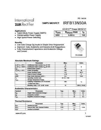
PD - 94339 SMPS MOSFET IRFB13N50A HEXFET Power MOSFET Applications VDSS RDS(on) max ID Switch Mode Power Supply (SMPS) Uninterruptible Power Supply 500V 0.450 14A High Speed Power Switching Benefits Low Gate Charge Qg results in Simple Drive Requirement Improved Gate, Avalanche and Dynamicdv/dt Ruggedness Fully Characterized Capacitance and Avalanche Voltage and Current... See More ⇒
std13n50dm2ag.pdf
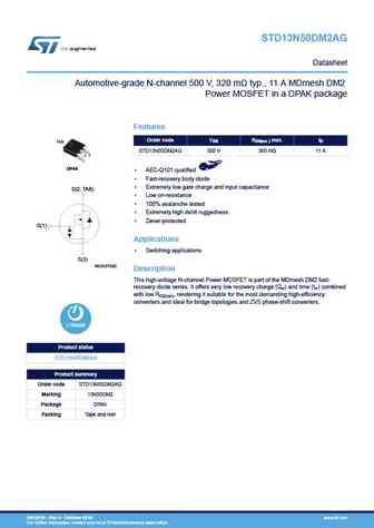
STD13N50DM2AG Datasheet Automotive-grade N-channel 500 V, 320 m typ., 11 A MDmesh DM2 Power MOSFET in a DPAK package Features VDS RDS(on ) max. ID Order code TAB STD13N50DM2AG 500 V 360 m 11 A 3 2 1 DPAK AEC-Q101 qualified Fast-recovery body diode Extremely low gate charge and input capacitance D(2, TAB) Low on-resistance 100% avalanche tested E... See More ⇒
fqb13n50ctm fqb13n50c fqi13n50c fqi13n50ctu.pdf
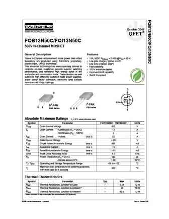
October 2008 QFET FQB13N50C/FQI13N50C 500V N-Channel MOSFET General Description Features These N-Channel enhancement mode power field effect 13A, 500V, RDS(on) = 0.48 @VGS = 10 V transistors are produced using Fairchild s proprietary, Low gate charge ( typical 43nC) planar stripe, DMOS technology. Low Crss ( typical 20pF) This advanced technology has been especially ... See More ⇒
fqa13n50c.pdf
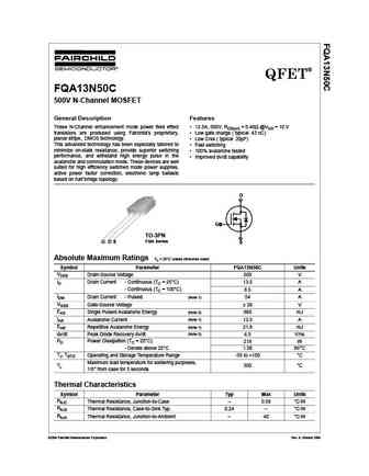
QFET FQA13N50C 500V N-Channel MOSFET General Description Features These N-Channel enhancement mode power field effect 13.5A, 500V, RDS(on) = 0.48 @VGS = 10 V transistors are produced using Fairchild s proprietary, Low gate charge ( typical 43 nC) planar stripe, DMOS technology. Low Crss ( typical 20pF) This advanced technology has been especially tailored to Fa... See More ⇒
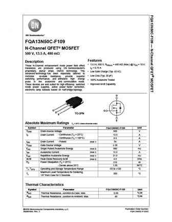
fqa13n50c f109.pdf
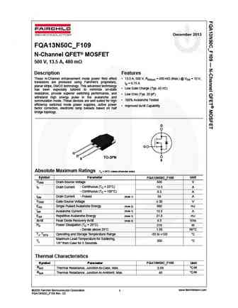
December 2013 FQA13N50C_F109 N-Channel QFET MOSFET 500 V, 13.5 A, 480 m Description Features These N-Channel enhancement mode power field effect 13.5 A, 500 V, RDS(on) = 480 m (Max.) @ VGS = 10 V, transistors are produced using Fairchild s proprietary, ID = 6.75 A planar stripe, DMOS technology. This advanced technology Low Gate Charge (Typ. 43 nC) has been especia... See More ⇒
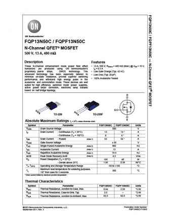
fqp13n50c fqpf13n50c.pdf
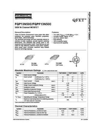
TM QFET FQP13N50C/FQPF13N50C 500V N-Channel MOSFET General Description Features These N-Channel enhancement mode power field effect 13A, 500V, RDS(on) = 0.48 @VGS = 10 V transistors are produced using Fairchild s proprietary, Low gate charge ( typical 43 nC) planar stripe, DMOS technology. Low Crss ( typical 20pF) This advanced technology has been especially tailored t... See More ⇒
fqp13n50cf fqpf13n50cf.pdf
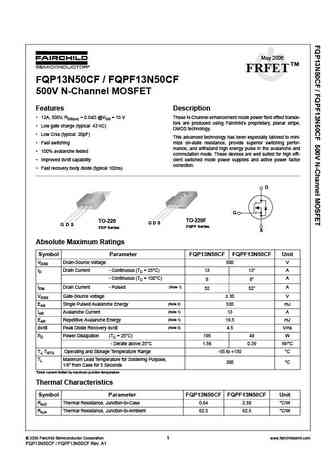
May 2006 TM FRFET FQP13N50CF / FQPF13N50CF 500V N-Channel MOSFET Features Description 13A, 500V, RDS(on) = 0.54 @VGS = 10 V These N-Channel enhancement mode power field effect transis- tors are produced using Fairchild s proprietary, planar stripe, Low gate charge (typical 43 nC) DMOS technology. Low Crss (typical 20pF) This advanced technology has been especially t... See More ⇒
fqp13n50c fqpf13n50c.pdf
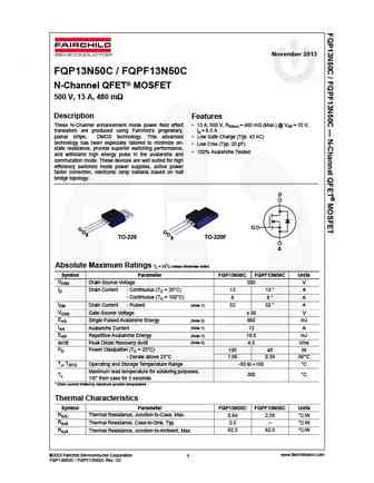
November 2013 FQP13N50C / FQPF13N50C N-Channel QFET MOSFET 500 V, 13 A, 480 m Description Features These N-Channel enhancement mode power field effect 13 A, 500 V, RDS(on) = 480 m (Max.) @ VGS = 10 V, transistors are produced using Fairchild s proprietary, ID = 6.5 A planar stripe, DMOS technology. This advanced Low Gate Charge (Typ. 43 nC) technology has been especia... See More ⇒
fqa13n50.pdf
April 2000 TM QFET QFET QFET QFET 500V N-ChanneI MOSFET GeneraI Description Features These N-Channel enhancement mode power field effect 13.4A, 500V, RDS(on) = 0.43 @VGS = 10 V transistors are produced using Fairchild s proprietary, Low gate charge ( typical 45 nC) planar stripe, DMOS technology. Low Crss ( typical 25 pF) This advanced technology has been... See More ⇒
fdp13n50f fdpf13n50ft.pdf
September 2007 UniFETTM FDP13N50F / FDPF13N50FT tm N-Channel MOSFET 500V, 12A, 0.54 Features Description RDS(on) = 0.42 ( Typ.)@ VGS = 10V, ID = 6A These N-Channel enhancement mode power field effect transistors are produced using Fairchild s proprietary, planar Low gate charge ( Typ. 30nC) stripe, DMOS technology. Low Crss ( Typ. 14.5pF) This advanced technol... See More ⇒
fqpf13n50 fqpf13n50t.pdf
TM QFET FQP13N50/FQPF13N50 500V N-Channel MOSFET General Description Features These N-Channel enhancement mode power field effect 12.5A, 500V, RDS(on) = 0.43 @VGS = 10 V transistors are produced using Fairchild s proprietary, Low gate charge ( typical 45 nC) planar stripe, DMOS technology. Low Crss ( typical 25 pF) This advanced technology has been especially tailored ... See More ⇒
fqa13n50cf.pdf
July 2007 FRFET FQA13N50CF 500V N-Channel MOSFET Features Description 15A, 500V, RDS(on) = 0.48 @VGS = 10 V These N-Channel enhancement mode power field effect Low gate charge (typical 43nC) transistors are produced using Fairchild s proprietary, planar stripe, DMOS technology. Low Crss (typical 20pF) This advanced technology has been especially tailored to ... See More ⇒
fqp13n50 fqpf13n50.pdf

TM QFET FQP13N50/FQPF13N50 500V N-Channel MOSFET General Description Features These N-Channel enhancement mode power field effect 12.5A, 500V, RDS(on) = 0.43 @VGS = 10 V transistors are produced using Fairchild s proprietary, Low gate charge ( typical 45 nC) planar stripe, DMOS technology. Low Crss ( typical 25 pF) This advanced technology has been especially tailored ... See More ⇒
fqpf13n50csdtu fqpf13n50ct.pdf

TM QFET FQP13N50C/FQPF13N50C 500V N-Channel MOSFET General Description Features These N-Channel enhancement mode power field effect 13A, 500V, RDS(on) = 0.48 @VGS = 10 V transistors are produced using Fairchild s proprietary, Low gate charge ( typical 43 nC) planar stripe, DMOS technology. Low Crss ( typical 20pF) This advanced technology has been especially tailored t... See More ⇒
irfb13n50a sihfb13n50a.pdf

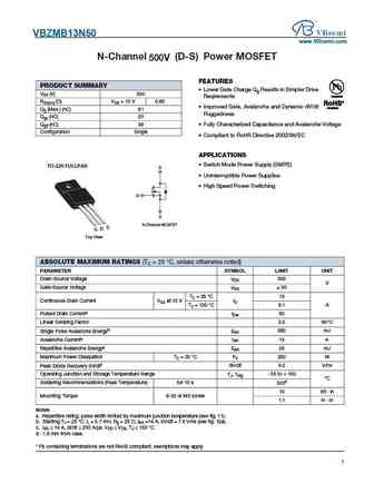
IRFB13N50A, SiHFB13N50A Vishay Siliconix Power MOSFET FEATURES PRODUCT SUMMARY Lower Gate Charge Qg Results in Simpler Drive VDS (V) 500 Reqirements Available RDS(on) ( )VGS = 10 V 0.450 RoHS* Improved Gate, Avalanche and Dynamic dV/dt Qg (Max.) (nC) 81 COMPLIANT Ruggedness Qgs (nC) 20 Qgd (nC) 36 Fully Characterized Capacitance and Avalanche Voltage Configuratio... See More ⇒
irfb13n50a irfb13n50apbf sihfb13n50a.pdf
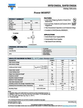
IRFB13N50A, SiHFB13N50A Vishay Siliconix Power MOSFET FEATURES PRODUCT SUMMARY Lower Gate Charge Qg Results in Simpler Drive VDS (V) 500 Reqirements Available RDS(on) ( )VGS = 10 V 0.450 RoHS* Improved Gate, Avalanche and Dynamic dV/dt Qg (Max.) (nC) 81 COMPLIANT Ruggedness Qgs (nC) 20 Qgd (nC) 36 Fully Characterized Capacitance and Avalanche Voltage Configuratio... See More ⇒
zxt13n50de6.pdf
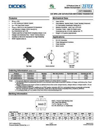
A Product Line of Diodes Incorporated ZXT13N50DE6 50V NPN LOW SATURATION SWITCHING TRANSISTOR Features Mechanical Data BVCEO > 50V Case SOT26 IC = 4A Continuous Collector Current Case Material Molded Plastic, Green Molding Compound. ICM = 10A Peak Pulse Current UL Flammability Classification Rating 94V-0 RCE(SAT) = 36m for a Low Equivalent On-Res... See More ⇒
irfb13n50a sihfb13n50a.pdf
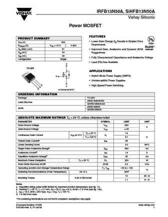
IRFB13N50A, SiHFB13N50A Vishay Siliconix Power MOSFET FEATURES PRODUCT SUMMARY Lower Gate Charge Qg Results in Simpler Drive VDS (V) 500 Available Reqirements RDS(on) ( )VGS = 10 V 0.450 RoHS* Qg (Max.) (nC) 81 Improved Gate, Avalanche and Dynamic dV/dt COMPLIANT Qgs (nC) 20 Ruggedness Qgd (nC) 36 Fully Characterized Capacitance and Avalanche Voltage Configuration... See More ⇒
ixfj13n50.pdf
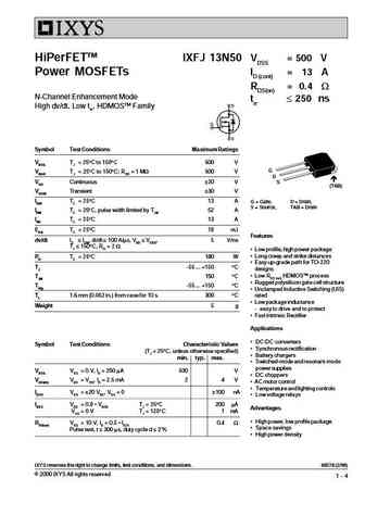
HiPerFETTM IXFJ 13N50 VDSS = 500 V Power MOSFETs ID (cont) = 13 A RDS(on) = 0.4 W N-Channel Enhancement Mode trr 250 ns High dv/dt, Low trr, HDMOSTM Family Symbol Test Conditions Maximum Ratings VDSS TJ = 25 C to 150 C 500 V G VDGR TJ = 25 C to 150 C; RGS = 1 MW 500 V D VGS Continuous 20 V S (TAB) VGSM Transient 30 V ID25 TC = 25 C13 A G = Gate, D = Drain, S = So... See More ⇒
ixfh13n50 ixfm13n50.pdf
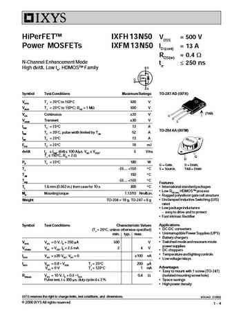
HiPerFETTM IXFH 13 N50 VDSS = 500 V Power MOSFETs IXFM 13 N50 ID (cont) = 13 A RDS(on) = 0.4 W N-Channel Enhancement Mode trr 250 ns High dv/dt, Low trr, HDMOSTM Family Symbol Test Conditions Maximum Ratings TO-247 AD (IXFH) VDSS TJ = 25 C to 150 C 500 V VDGR TJ = 25 C to 150 C; RGS = 1 MW 500 V (TAB) VGS Continuous 20 V VGSM Transient 30 V ID25 TC = 25 C13 A TO-204 AA ... See More ⇒
fqp13n50c fqpf13n50c.pdf
FQP13N50C / FQPF13N50C N-Channel QFET MOSFET 500 V, 13 A, 480 m Description Features These N-Channel enhancement mode power field effect 13 A, 500 V, RDS(on) = 480 m (Max.) @ VGS = 10 V, transistors are produced using ON Semiconductor s ID = 6.5 A proprietary, planar stripe, DMOS technology. This Low Gate Charge (Typ. 43 nC) advanced technology has been especially tail... See More ⇒
fqa13n50cf.pdf

Is Now Part of To learn more about ON Semiconductor, please visit our website at www.onsemi.com Please note As part of the Fairchild Semiconductor integration, some of the Fairchild orderable part numbers will need to change in order to meet ON Semiconductor s system requirements. Since the ON Semiconductor product management systems do not have the ability to manage part nomenclatur... See More ⇒
fqi13n50c.pdf

Is Now Part of To learn more about ON Semiconductor, please visit our website at www.onsemi.com Please note As part of the Fairchild Semiconductor integration, some of the Fairchild orderable part numbers will need to change in order to meet ON Semiconductor s system requirements. Since the ON Semiconductor product management systems do not have the ability to manage part nomenclatur... See More ⇒
fqpf13n50cf.pdf

Is Now Part of To learn more about ON Semiconductor, please visit our website at www.onsemi.com Please note As part of the Fairchild Semiconductor integration, some of the Fairchild orderable part numbers will need to change in order to meet ON Semiconductor s system requirements. Since the ON Semiconductor product management systems do not have the ability to manage part nomenclatur... See More ⇒
fqp13n50 fqpf13n50.pdf

TM QFET FQP13N50/FQPF13N50 500V N-Channel MOSFET General Description Features These N-Channel enhancement mode power field effect 12.5A, 500V, RDS(on) = 0.43 @VGS = 10 V transistors are produced using Fairchild s proprietary, Low gate charge ( typical 45 nC) planar stripe, DMOS technology. Low Crss ( typical 25 pF) This advanced technology has been especially tailored ... See More ⇒
fqa13n50c-f109.pdf
ON Semiconductor and are trademarks of Semiconductor Components Industries, LLC dba ON Semiconductor or its subsidiaries in the United States and/or other countries. ON Semiconductor owns the rights to a number of patents, trademarks, copyrights, trade secrets, and other intellectual property. A listing of ON Semiconductor s product/patent coverage may be accessed at www.onsemi.com/s... See More ⇒
13n50.pdf
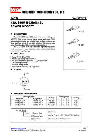
UNISONIC TECHNOLOGIES CO., LTD 13N50 Power MOSFET 13A, 500V N-CHANNEL POWER MOSFET 1 TO-220 DESCRIPTION The UTC 13N50 is an N-Channel enhancement mode power MOSFET. The device adopts planar stripe and uses DMOS technology to minimize and provide lower on-state resistance and faster switching speed. It can also withstand high energy pulse 1 under the avalanche and commutat... See More ⇒
tsm13n50ci tsm13n50cz.pdf
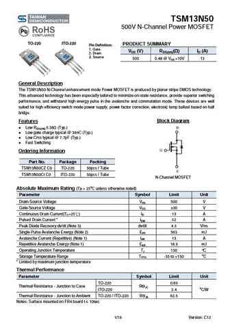
TSM13N50 500V N-Channel Power MOSFET TO-220 ITO-220 PRODUCT SUMMARY Pin Definition 1. Gate VDS (V) RDS(on)( ) ID (A) 2. Drain 3. Source 500 0.48 @ VGS =10V 13 General Description The TSM13N50 N-Channel enhancement mode Power MOSFET is produced by planar stripe DMOS technology. This advanced technology has been especially tailored to minimize on-state resistance, prov... See More ⇒
kf13n50p-f.pdf
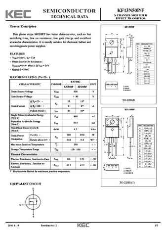
KF13N50P/F SEMICONDUCTOR N CHANNEL MOS FIELD TECHNICAL DATA EFFECT TRANSISTOR General Description KF13N50P This planar stripe MOSFET has better characteristics, such as fast switching time, low on resistance, low gate charge and excellent avalanche characteristics. It is mainly suitable for electronic ballast and switching mode power supplies. FEATURES VDSS= 500V, ID= 13A Dra... See More ⇒
aot13n50 aotf13n50.pdf
AOT13N50/AOTF13N50 500V, 13A N-Channel MOSFET General Description Product Summary VDS 600V@150 The AOT13N50 & AOTF13N50 have been fabricated using an advanced high voltage MOSFET process that is ID (at VGS=10V) 13A designed to deliver high levels of performance and RDS(ON) (at VGS=10V) ... See More ⇒
aot13n50.pdf
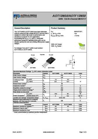
AOT13N50/AOTF13N50 500V, 13A N-Channel MOSFET General Description Product Summary VDS 600V@150 The AOT13N50 & AOTF13N50 have been fabricated using an advanced high voltage MOSFET process that is ID (at VGS=10V) 13A designed to deliver high levels of performance and RDS(ON) (at VGS=10V) ... See More ⇒
aotf13n50.pdf

AOT13N50/AOTF13N50 500V, 13A N-Channel MOSFET General Description Product Summary VDS 600V@150 The AOT13N50 & AOTF13N50 have been fabricated using an advanced high voltage MOSFET process that is ID (at VGS=10V) 13A designed to deliver high levels of performance and RDS(ON) (at VGS=10V) ... See More ⇒
ap13n50r-hf.pdf
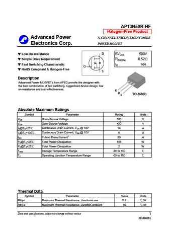
AP13N50R-HF Halogen-Free Product Advanced Power N-CHANNEL ENHANCEMENT MODE Electronics Corp. POWER MOSFET D Low On-resistance BVDSS 500V Simple Drive Requirement RDS(ON) 0.52 Fast Switching Characteristic ID 14A G RoHS Compliant & Halogen-Free S Description Advanced Power MOSFETs from APEC provide the designer with the best combination of fast switching, ruggedize... See More ⇒
ap13n50w.pdf
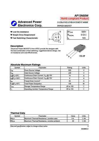
AP13N50W RoHS-compliant Product Advanced Power N-CHANNEL ENHANCEMENT MODE Electronics Corp. POWER MOSFET D Low On-resistance BVDSS 500V Simple Drive Requirement RDS(ON) 0.52 Fast Switching Characteristic ID 14A G S Description Advanced Power MOSFETs from APEC provide the designer with the best combination of fast switching, ruggedized device design, low on-resistance ... See More ⇒
ap13n50r.pdf
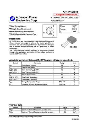
AP13N50R-HF Halogen-Free Product Advanced Power N-CHANNEL ENHANCEMENT MODE Electronics Corp. POWER MOSFET D Low On-resistance BVDSS 500V Simple Drive Requirement RDS(ON) 0.52 Fast Switching Characteristic ID 14A G RoHS Compliant & Halogen-Free S Description AP13N50 series are from Advanced Power innovated design and silicon process technology to achieve the lowest... See More ⇒
ap13n50i-hf.pdf
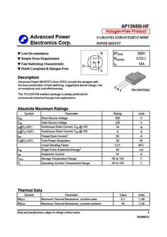
AP13N50I-HF Halogen-Free Product Advanced Power N-CHANNEL ENHANCEMENT MODE Electronics Corp. POWER MOSFET D Low On-resistance BVDSS 500V Simple Drive Requirement RDS(ON) 0.52 Fast Switching Characteristic ID 14A G RoHS Compliant & Halogen-Free S Description Advanced Power MOSFETs from APEC provide the designer with the best combination of fast switching, ruggedize... See More ⇒
sif13n50c.pdf
Shenzhen SI Semiconductors Co., LTD. Product Specification Shenzhen SI Semiconductors Co., LTD. Product Specification Shenzhen SI Semiconductors Co., LTD. Product Specification Shenzhen SI Semiconductors Co., LTD. Product Specification N- MOS / N-CHANNEL POWER MOSFET SIF13N50C N- MOS / N-CHANNEL POWER MOSFET SIF13N50C N- MOS / N-CHA... See More ⇒
jcs13n50ft.pdf
N N- CHANNEL MOSFET R JCS13N50FT MAIN CHARACTERISTICS Package ID 13 A VDSS 500 V Rdson-max @Vgs=10V 0.46 Qg-typ 37 nC APPLICATIONS High frequency switching mode power supply UPS Electronic ballast UPS FEATUR... See More ⇒
mtn13n50e3.pdf
Spec. No. C405E3 Issued Date 2008.12.01 CYStech Electronics Corp. Revised Date 2009.08.13 Page No. 1/8 N-Channel Enhancement Mode Power MOSFET BVDSS 500V RDS(ON) 0.48 MTN13N50E3 ID 13A Description The MTN13N50E3 is a N-channel enhancement-mode MOSFET, providing the designer with the best combination of fast switching, ruggedized device design, low on-resis... See More ⇒
mtn13n50fp.pdf
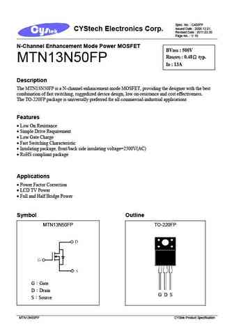
Spec. No. C405FP Issued Date 2008.12.01 CYStech Electronics Corp. Revised Date 2011.03.30 Page No. 1/ 10 N-Channel Enhancement Mode Power MOSFET BVDSS 500V RDS(ON) 0.48 typ. MTN13N50FP ID 13A Description The MTN13N50FP is a N-channel enhancement-mode MOSFET, providing the designer with the best combination of fast switching, ruggedized device design, low o... See More ⇒
13n50.pdf
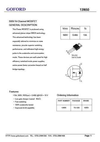
GOFORD 13N50 500V N-Channel MOSFET GENERAL DESCRIPTION VDSS RDS(ON) ID This Power MOSFET is produced using advanced planar stripe DMOS technology. 500V 0.48 13A This advanced technology has been especially tailored to minimize on-state resistance, provide superior switching performance, and withstand high energy pulse in the avalanche and commutation mode. These devices are well ... See More ⇒
ssf13n50.pdf
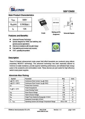
SSF13N50 Main Product Characteristics VDSS 500V RDS(on) 0.39 (typ.) ID 13A Marking and Pin TO-220 Schematic Diagram Assignment Features and Benefits Advanced Process Technology Special designed for PWM, load switching and general purpose applications Ultra low on-resistance with low gate charge Fast switching and reverse body recovery 150 o... See More ⇒
ssf13n50f.pdf
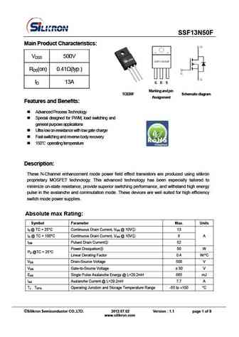
SSF13N50F Main Product Characteristics VDSS 500V RDS(on) 0.41 (typ.) ID 13A Marking a nd p in Sche ma ti c di agr a m TO220F Assignment Features and Benefits Advanced Process Technology Special designed for PWM, load switching and general purpose applications Ultra low on-resistance with low gate charge Fast switching and reverse body recovery ... See More ⇒
br13n50.pdf
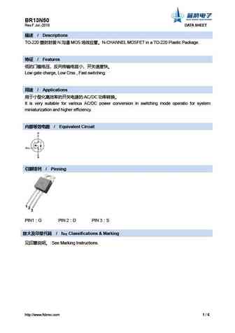
BR13N50 Rev.F Jul.-2018 DATA SHEET / Descriptions TO-220 N MOS N-CHANNEL MOSFET in a TO-220 Plastic Package. / Features Low gate charge, Low Crss , Fast switching. / Applications AC/DC It is very suit... See More ⇒
brb13n50.pdf
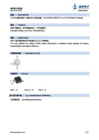
BRB13N50 Rev.A Nov.-2016 DATA SHEET / Descriptions TO-263 N MOS N-CHANNEL MOSFET in a TO-263Plastic Package. / Features Low gate charge, Low Crss , Fast switching. / Applications AC/DC It is very suit... See More ⇒
brf13n50.pdf
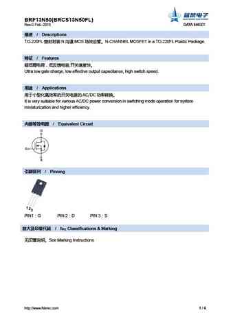
BRF13N50(BRCS13N50FL) Rev.C Feb.-2015 DATA SHEET / Descriptions TO-220FL N MOS N-CHANNEL MOSFET in a TO-220FL Plastic Package. / Features , Ultra low gate charge, low effective output capacitance, high switch speed. / Applications ... See More ⇒
brfl13n50.pdf
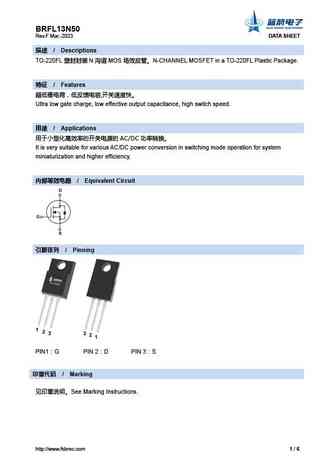
BRFL13N50 Rev.F Mar.-2023 DATA SHEET / Descriptions TO-220FL N MOS N-CHANNEL MOSFET in a TO-220FL Plastic Package. / Features , Ultra low gate charge, low effective output capacitance, high switch speed. / Applications AC/DC ... See More ⇒
irf13n50.pdf
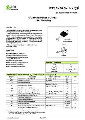
RoHS IRF13N50 Series RoHS SEMICONDUCTOR Nell High Power Products N-Channel Power MOSFET (14A, 500Volts) DESCRIPTION The Nell IRF13N50 are N-channel enhancement mode D silicon gate power field effect transistors. They are designed, tested and guaranteed to withstand level of energy in breakdown avalanche made of operation. They are designed as an extremely efficient and reliab... See More ⇒
hfp13n50.pdf
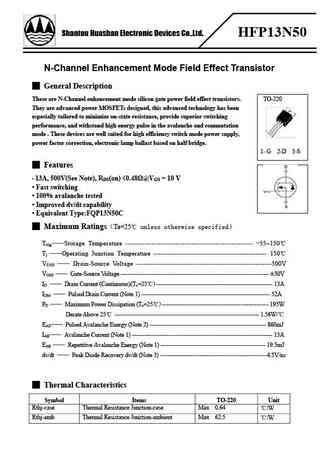
Shantou Huashan Electronic Devices Co.,Ltd. HFP13N50 N-Channel Enhancement Mode Field Effect Transistor General Description These are N-Channel enhancement mode silicon gate power field effect transistors. TO-220 They are advanced power MOSFETs designed, this advanced technology has been especially tailored to minimize on-state resistance, provide superior switching performan... See More ⇒
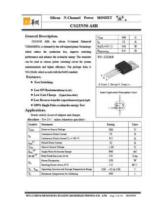
cs13n50 a8d.pdf
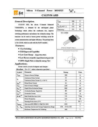
Silicon N-Channel Power MOSFET R CS13N50 A8D VDSS 500 V General Description ID 13 A CS13N50 A8D, the silicon N-channel Enhanced PD (TC=25 ) 125 W VDMOSFETs, is obtained by the self-aligned planar RDS(ON)Typ 0.4 Technology which reduce the conduction loss, improve switching performance and enhance the avalanche energy. The transistor can be used in various ... See More ⇒
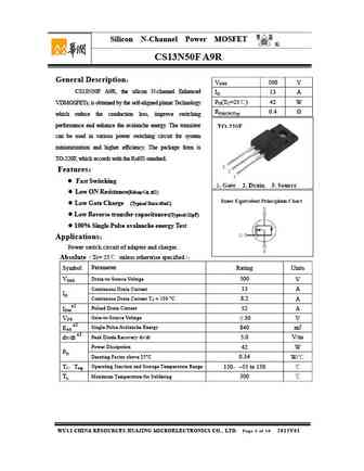
cs13n50f a9d.pdf
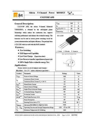
Silicon N-Channel Power MOSFET R CS13N50F A9D VDSS 500 V General Description ID 13 A CS13N50F A9D, the silicon N-channel Enhanced PD (TC=25 ) 60 W VDMOSFETs, is obtained by the self-aligned planar RDS(ON)Typ 0.4 Technology which reduce the conduction loss, improve switching performance and enhance the avalanche energy. The transistor can be used in various po... See More ⇒
cs13n50 a8r.pdf
Silicon N-Channel Power MOSFET R CS13N50 A8R General Description VDSS 500 V CS13N50 A8R, the silicon N-channel Enhanced ID 13 A PD(TC=25 ) 150 W VDMOSFETs, is obtained by the self-aligned planar Technology RDS(ON)Typ 0.4 which reduce the conduction loss, improve switching performance and enhance the avalanche energy. The transistor can be used in various pow... See More ⇒
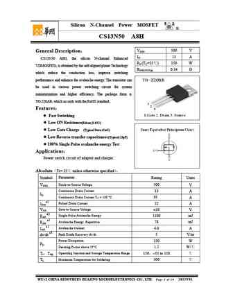
cs13n50 a8h.pdf

Silicon N-Channel Power MOSFET R CS13N50 A8H VDSS 500 V General Description ID 13 A CS13N50 A8H, the silicon N-channel Enhanced PD (TC=25 ) 150 W VDMOSFETs, is obtained by the self-aligned planar Technology RDS(ON)Typ 0.34 which reduce the conduction loss, improve switching performance and enhance the avalanche energy. The transistor can be used in various p... See More ⇒
cs13n50f a9r.pdf

Silicon N-Channel Power MOSFET R CS13N50F A9R General Description VDSS 500 V CS13N50F A9R, the silicon N-channel Enhanced ID 13 A PD(TC=25 ) 42 W VDMOSFETs, is obtained by the self-aligned planar Technology RDS(ON)Typ 0.4 which reduce the conduction loss, improve switching performance and enhance the avalanche energy. The transistor can be used in various po... See More ⇒
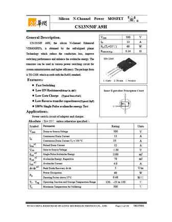
cs13n50f a9h.pdf

Silicon N-Channel Power MOSFET R CS13N50F A9H VDSS 500 V General Description ID 13 A CS13N50F A9H, the silicon N-channel Enhanced PD (TC=25 ) 60 W VDMOSFETs, is obtained by the self-aligned planar RDS(ON)Typ 0.34 Technology which reduce the conduction loss, improve switching performance and enhance the avalanche energy. The transistor can be used in variou... See More ⇒
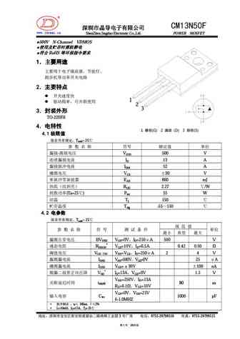
cm13n50.pdf
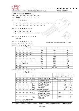
R C1N0 M35 www.jdsemi.cn ShenZhen Jingdao Electronic Co.,Ltd. POWER MOSFET 500V N-Channel VDMOS RoHS 1 2 3 ... See More ⇒
e13n50.pdf
E13N50 13A 500V N-channel Enhancement Mode Power MOSFET 1 Description These N-channel enhanced vdmosfets, is obtained by the self-aligned V DSS = 500V planar technology which reduce the conduction loss, improve switching I = 13.0A D performance and enhance the avalanche energy. Which accords with the RoHS standard. R DS(on) TYP) =0.35 2 Features Fast switching ESD im... See More ⇒
f13n50.pdf
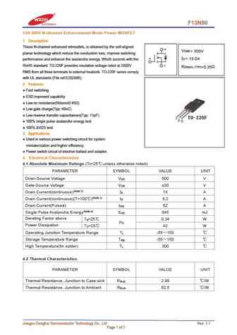
F13N50 13A 500V N-channel Enhancement Mode Power MOSFET 1 Description These N-channel enhanced vdmosfets, is obtained by the self-aligned V DSS = 500V planar technology which reduce the conduction loss, improve switching I = 13.0A D performance and enhance the avalanche energy. Which accords with the RoHS standard. TO-220F provides insulation voltage rated at 2000V R DS(on) TYP) ... See More ⇒
13n50.pdf
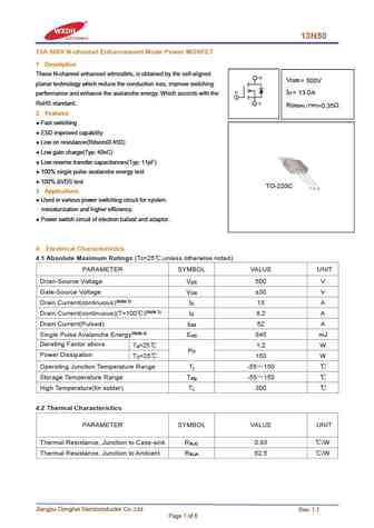
13N50 13A 500V N-channel Enhancement Mode Power MOSFET 1 Description These N-channel enhanced vdmosfets, is obtained by the self-aligned V DSS = 500V planar technology which reduce the conduction loss, improve switching I = 13.0A D performance and enhance the avalanche energy. Which accords with the RoHS standard. R DS(on) TYP) =0.35 2 Features Fast switching ESD imp... See More ⇒
mdp13n50th.pdf
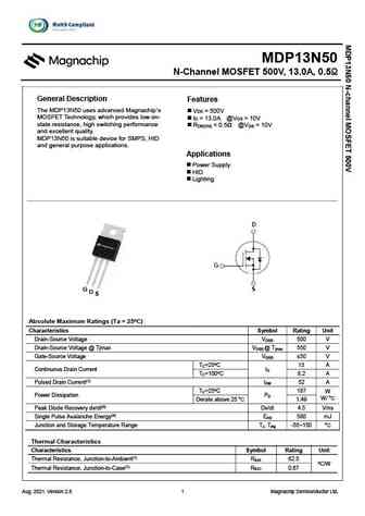
MDP13N50 N-Channel MOSFET 500V, 13.0A, 0.5 General Description Features The MDP13N50 uses advanced Magnachip s V = 500V DS MOSFET Technology, which provides low on- I = 13.0A @V = 10V D GS state resistance, high switching performance R ... See More ⇒
mdf13n50gth mdp13n50gth.pdf
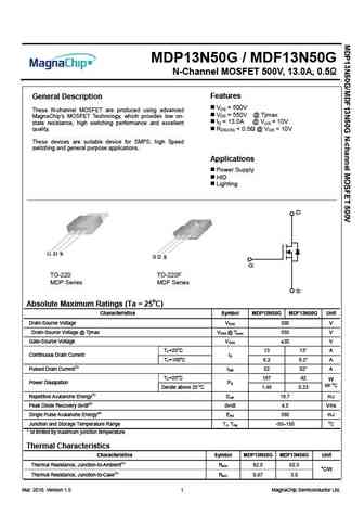
MDP13N50G / MDF13N50G N-Channel MOSFET 500V, 13.0A, 0.5 General Description Features VDS = 500V These N-channel MOSFET are produced using advanced VDS = 550V @ Tjmax MagnaChip s MOSFET Technology, which provides low on- ID = 13.0A @ VGS = 10V state resistance, high switching performance and excellent RDS(ON) ... See More ⇒
mdf13n50bth mdp13n50bth.pdf
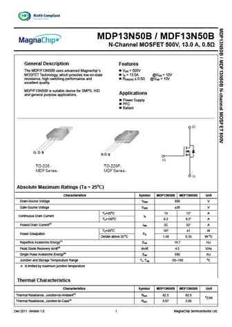
MDP13N50B / MDF13N50B N-Channel MOSFET 500V, 13.0 A, 0.5 General Description Features The MDP/F13N50B uses advanced Magnachip s VDS = 500V MOSFET Technology, which provides low on-state ID = 13.0A @VGS = 10V resistance, high switching performance and RDS(ON) 0.5 @VGS = 10V excellent quality. MDP/F13N50B is suitable device for SMPS, HID Applications and general p... See More ⇒
msf13n50.pdf
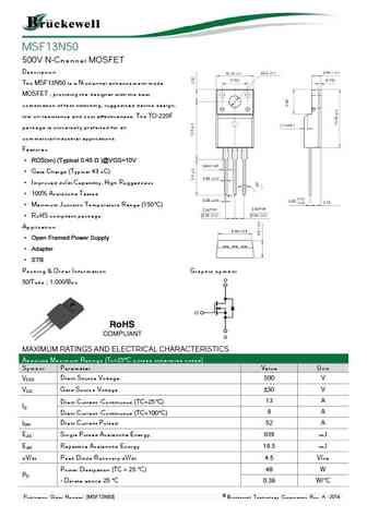
MSF13N50 500V N-Channel MOSFET Description The MSF13N50 is a N-channel enhancement-mode MOSFET , providing the designer with the best combination of fast switching, ruggedized device design, low on-resistance and cost effectiveness. The TO-220F package is universally preferred for all commercial-industrial applications Features RDS(on) (Typical 0.48 )@VGS=10V Ga... See More ⇒
ms13n50.pdf
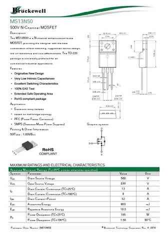
MS13N50 500V N-Channel MOSFET Description The MS13N50 is a N-channel enhancement-mode MOSFET, providing the designer with the best combination of fast switching, ruggedized device design, low on-resistance and cost effectiveness. The TO-220 package is universally preferred for all commercial-industrial applications Features Originative New Design Very Low Intrinsic... See More ⇒
wfp13n50.pdf
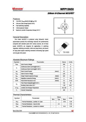
WFP13N50 WFP13N50 WFP13N50 WFP13N50 Silicon N-Channel MOSFET Silicon N-Channel MOSFET Silicon N-Channel MOSFET Silicon N-Channel MOSFET Features 13A,500V, R (Max0.46 )@V =10V DS(on) GS Ultra-low Gate charge(Typical 43nC) Fast Switching Capability 100%Avalanche Tested Maximum Junction Temperature Range(150 ) General Description This Power MOSFET is produce... See More ⇒
wff13n50.pdf
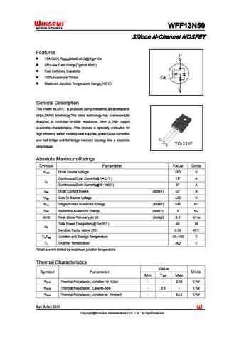
WFF13N50 WFF13N50 WFF13N50 WFF13N50 Silicon N-Channel MOSFET Silicon N-Channel MOSFET Silicon N-Channel MOSFET Silicon N-Channel MOSFET Features 13A,500V, R (Max0.46 )@V =10V DS(on) GS Ultra-low Gate charge(Typical 43nC) Fast Switching Capability 100%Avalanche Tested Maximum Junction Temperature Range(150 ) General Description This Power MOSFET is produce... See More ⇒
wfw13n50.pdf
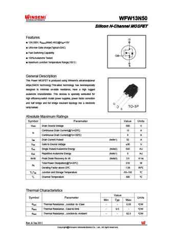
WFW13N50 WFW13N50 WFW13N50 WFW13N50 Silicon N-Channel MOSFET Silicon N-Channel MOSFET Silicon N-Channel MOSFET Silicon N-Channel MOSFET Features 13A,500V, R (Max0.46 )@V =10V DS(on) GS Ultra-low Gate charge(Typical 43nC) Fast Switching Capability 100%Avalanche Tested Maximum Junction Temperature Range(150 ) General Description This Power MOSFET is produce... See More ⇒
sfp13n50.pdf
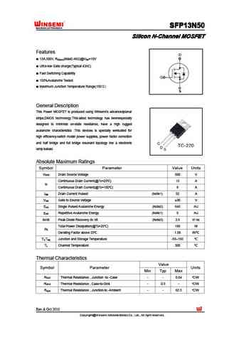
SFP13N50 SFP13N50 SFP13N50 SFP13N50 Silicon N-Channel MOSFET Silicon N-Channel MOSFET Silicon N-Channel MOSFET Silicon N-Channel MOSFET Features 13A,500V, R (Max0.46 )@V =10V DS(on) GS Ultra-low Gate charge(Typical 43nC) Fast Switching Capability 100%Avalanche Tested Maximum Junction Temperature Range(150 ) General Description This Power MOSFET is produce... See More ⇒
bl13n50-p bl13n50-a.pdf
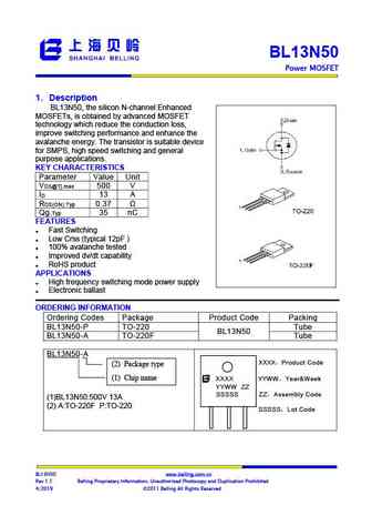
BL13N50 Power MOSFET 1 Description BL13N50, the silicon N-channel Enhanced MOSFETs, is obtained by advanced MOSFET technology which reduce the conduction loss, improve switching performance and enhance the avalanche energy. The transistor is suitable device for SMPS, high speed switching and general purpose applications. KEY CHARACTERISTICS Parameter Value Unit V 500 V... See More ⇒
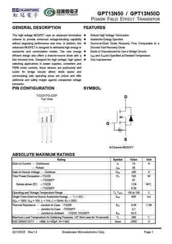
gpt13n50 gpt13n50d.pdf
GPT13N50 / GPT13N50D POWER FIELD EFFECT TRANSISTOR Fig 6. Typical Capacitance Vs. Fig 6. Typical Gate Charge Vs. Gate-to-Source Voltage Drain-to-Source Voltage 2013/6/26 Rev1.4 Greatpower Microelectronic Corp. Page 4 GPT13N50 / GPT13N50D POWER FIELD EFFECT TRANSISTOR PACKAGE DIMENSION TO-220 TO-220F 2013/6/26 Rev1.4 Greatpower Microelectronic Corp. Page 5 GPT13N50 / G... See More ⇒
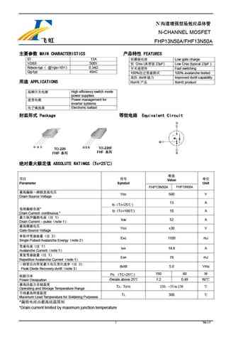
fhp13n50a fhf13n50a.pdf
N N-CHANNEL MOSFET FHP13N50A/FHF13N50A MAIN CHARACTERISTICS FEATURES ID 13A Low gate charge VDSS 500V Crss ( 23pF) Low Crss (typical 23pF ) Rdson-typ @Vgs=10V 0.34 Fast switching Qg-typ 45nC 100% 100% avalanche tested dv/dt Imp... See More ⇒
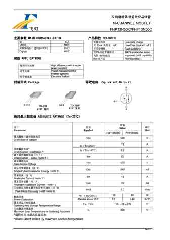
fhp13n50c fhf13n50c.pdf
N N-CHANNEL MOSFET FHP13N50C/FHF13N50C MAIN CHARACTERISTICS FEATURES ID 13A Low gate charge VDSS 500V Crss ( 11pF) Low Crss (typical 11pF ) Rdson-typ @Vgs=10V 0.4 Fast switching Qg-typ 40nC 100% 100% avalanche tested dv/dt Impr... See More ⇒
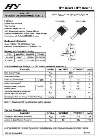
hy13n50t.pdf
HY13N50T / HY13N50FT 500V / 13A 500V, RDS(ON)=0.52W@VGS=10V, ID=6.5A N-Channel Enhancement Mode MOSFET Features TO-220AB ITO-220AB Low On-State Resistance Fast Switching Low Gate Charge & Low CRSS Fully Characterized Avalanche Voltage and Current Specially Desigened for AC Adapter, Battery Charger and SMPS In compliance with EU RoHs 2002/95/EC Directives 1... See More ⇒
jffm13n50e.pdf
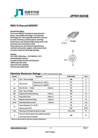
JFFM13N50E 500V N-Channel MOSFET General Description This Power MOSFET is produced using advanced planar stripe DMOS technology. This advanced technology has been especially tailored to minimize on-state resistance, provide superior switching performance, and withstand high energy pulse in the avalanche and commutation mode. These devices are well suited for high efficiency ... See More ⇒
jfpc13n50c jffm13n50c.pdf
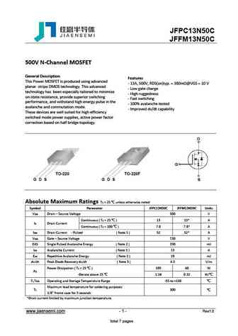
JFPC13N50C JFFM13N50C 500V N-Channel MOSFET General Description Features This Power MOSFET is produced using advanced - 13A, 500V, RDS(on)typ. = 380m @VGS = 10 V planar stripe DMOS technology. This advanced - Low gate charge technology has been especially tailored to minimize - High ruggedness on-state resistance, provide superior switching - Fast switching performanc... See More ⇒
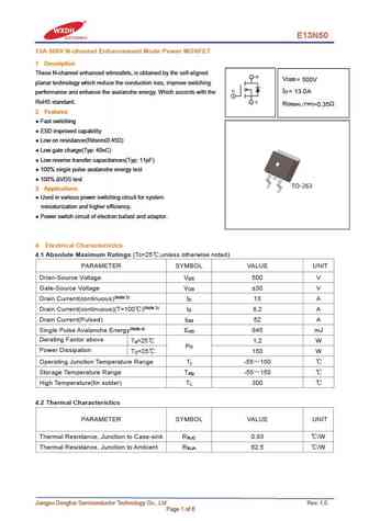
kia13n50h.pdf
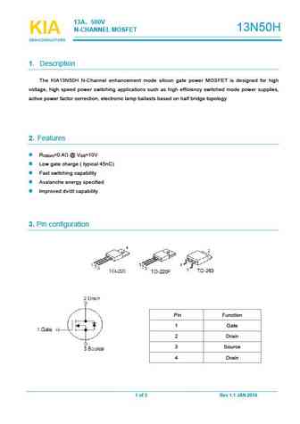
13A 500V 13N50H N-CHANNELMOSFET KIA KIA KIA SEMICONDUCTORS SEMICONDUCTORS SEMICONDUCTORS 1. Description The KIA13N50H N-Channel enhancement mode silicon gate power MOSFET is designed for high voltage, high speed power switching applications such as high efficiency switched mode power supplies, active power factor correction, electronic lamp ballasts based on half bridge topology ... See More ⇒
slp13n50a slf13n50a.pdf
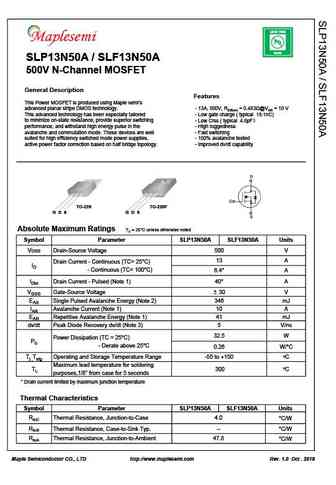
LEAD FREE Pb RoHS SLP13N50A / SLF13N50A 500V N-Channel MOSFET General Description Features This Power MOSFET is produced using Maple semi s advanced planar stripe DMOS technology. - 13A, 500V, RDS(on) = 0.483 @VGS = 10 V This advanced technology has been especially tailored - Low gate charge ( typical 19.1nC) to minimize on-state resistance, provide superior switching - Low Crss (... See More ⇒
sli13n50c.pdf
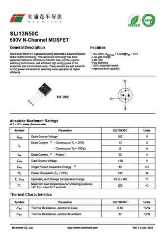
SLI13N50C 500V N-Channel MOSFET General Description Features This Power MOSFET is produced using Msemitek s advanced planar - 13A, 500V, RDS(on)typ = 0.48 @VGS = 10 V stripe DMOS technology. This advanced technology has been - Low gate charge especially tailored to minimize conduction loss, provide superior - Low Crss - Fast switching switching performance, and withstand high ener... See More ⇒
slp13n50c slf13n50c.pdf
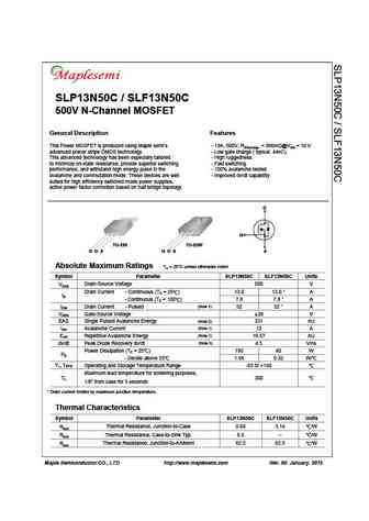
SLP13N50C / SLF13N50C 500V N-Channel MOSFET General Description Features This Power MOSFET is produced using Maple semi s - 13A, 500V, RDS(on)typ. = 386m @VGS = 10 V advanced planar stripe DMOS technology. - Low gate charge ( typical 44nC) This advanced technology has been especially tailored - High ruggedness to minimize on-state resistance, provide superior switching - Fast switching... See More ⇒
ptp13n50b pta13n50b.pdf
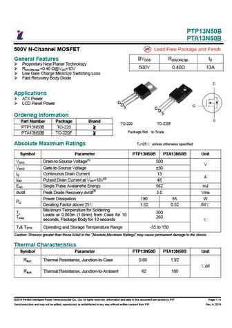
PTP13N50B PTA13N50B 500V N-Channel MOSFET General Features BVDSS RDS(ON),typ. ID Proprietary New Planar Technology 500V 0.40 13A RDS(ON),typ.=0.40 @VGS=10V Low Gate Charge Minimize Switching Loss Fast Recovery Body Diode Applications ATX Power G LCD Panel Power D S G D S Ordering Information Part Number Package Brand TO-220 TO-220F PTP13N50B TO-... See More ⇒
psa13n50 psp13n50.pdf
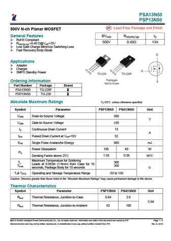
PSA13N50 PSP13N50 500V N-ch Planar MOSFET General Features BVDSS RDS(ON),Typ. ID RoHS Compliant 500V 0.40 13A RDS(ON),typ.=0.40 @VGS=10V Low Gate Charge Minimize Switching Loss Fast Recovery Body Diode Applications Adaptor Charger SMPS Standby Power Ordering Information Part Number Package Brand PSA13N50 TO-220F PSP13N50 TO-220 ... See More ⇒
swf13n50d swp13n50d.pdf
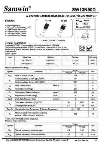
SW13N50D N-channel Enhancement mode TO-220F/TO-220 MOSFET TO-220F BVDSS 500V Features TO-220 ID 13A High ruggedness RDS(ON) 0.46 RDS(ON) (Typ 0.46 )@VGS=10V Gate Charge (Typ 47nC) 2 Improved dv/dt Capability 100% Avalanche Tested 1 1 2 2 Application LED,Charger 3 3 1 1. Gate 2. Drain 3. Source 3 General Description Thi... See More ⇒
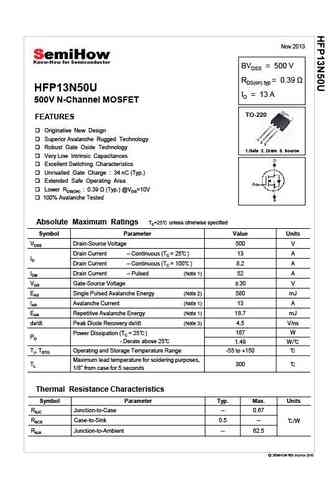
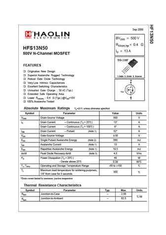
hfs13n50u.pdf
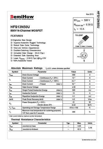
Nov 2013 BVDSS = 500 V RDS(on) typ = 0.39 HFS13N50U ID = 13 A 500V N-Channel MOSFET TO-220F FEATURES Originative New Design Superior Avalanche Rugged Technology 1 2 3 Robust Gate Oxide Technology 1.Gate 2. Drain 3. Source Very Low Intrinsic Capacitances Excellent Switching Characteristics Unrivalled Gate Charge 34 nC (Typ.) Extended Safe Operating Area Lo... See More ⇒
hfp13n50s.pdf
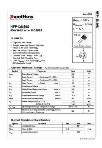
March 2014 BVDSS = 500 V RDS(on) typ HFP13N50S ID = 13 A 500V N-Channel MOSFET TO-220 FEATURES Originative New Design 1 2 3 Superior Avalanche Rugged Technology 1.Gate 2. Drain 3. Source Robust Gate Oxide Technology Very Low Intrinsic Capacitances Excellent Switching Characteristics Unrivalled Gate Charge 38 nC (Typ.) Extended Safe Operating Area L... See More ⇒
hfs13n50s.pdf
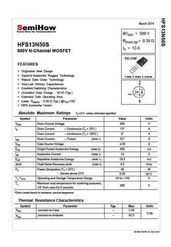
March 2014 BVDSS = 500 V RDS(on) typ HFS13N50S ID = 13 A 500V N-Channel MOSFET TO-220F FEATURES 1 Originative New Design 2 3 Superior Avalanche Rugged Technology 1.Gate 2. Drain 3. Source Robust Gate Oxide Technology Very Low Intrinsic Capacitances Excellent Switching Characteristics Unrivalled Gate Charge 38 nC (Typ.) Extended Safe Operating Area ... See More ⇒
hfp13n50u.pdf
Nov 2013 BVDSS = 500 V RDS(on) typ = 0.39 HFP13N50U ID = 13 A 500V N-Channel MOSFET TO-220 FEATURES Originative New Design Superior Avalanche Rugged Technology 1 2 3 Robust Gate Oxide Technology 1.Gate 2. Drain 3. Source Very Low Intrinsic Capacitances Excellent Switching Characteristics Unrivalled Gate Charge 34 nC (Typ.) Extended Safe Operating Area Low... See More ⇒
wvm13n50.pdf
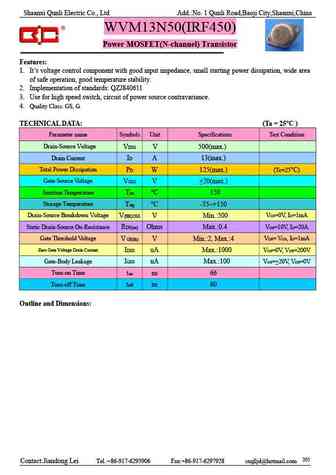
Shaanxi Qunli Electric Co., Ltd Add. No. 1 Qunli Road,Baoji City,Shaanxi,China WVM13N50(IRF450) Power MOSFET(N-channel) Transistor Features 1. It s voltage control component with good input impedance, small starting power dissipation, wide area of safe operation, good temperature stability. 2. Implementation of standards QZJ840611 3. Use for high speed switch, circuit of power s... See More ⇒
sl13n50fs.pdf
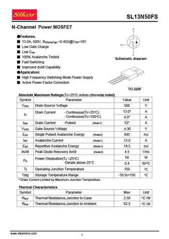
SL13N50FS N-Channel Power MOSFET Features 13.0A, 500V, R =0.40 @V =10V DS(on)(Typ) GS Low Gate Charge Low C rss 100% Avalanche Tested Schematic diagram Fast Switching Improved dv/dt Capability Application High Frequency Switching Mode Power Supply Active Power Factor Correction TO-220F Absolute Maximum Ratings(Tc=25 C unless otherw... See More ⇒
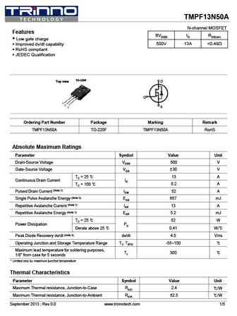
tmp13n50 tmpf13n50.pdf
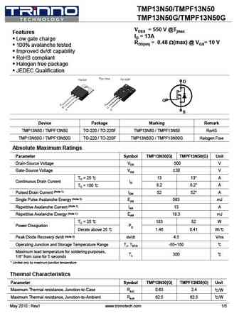
TMP13N50/TMPF13N50 TMP13N50G/TMPF13N50G VDSS = 550 V @Tjmax Features ID = 13A Low gate charge RDS(on) = 0.48 W(max) @ VGS= 10 V 100% avalanche tested Improved dv/dt capability RoHS compliant Halogen free package JEDEC Qualification D G S Device Package Marking Remark TMP13N50 / TMPF13N50 TO-220 / TO-220F TMP13N50 / TMPF13N50 RoHS TMP13N50G / TMPF13N50G... See More ⇒
tmpf13n50a.pdf
TMPF13N50A N-channel MOSFET Features BVDSS ID RDS(on) Low gate charge 500V 13A ... See More ⇒
tsp13n50m tsf13n50m.pdf
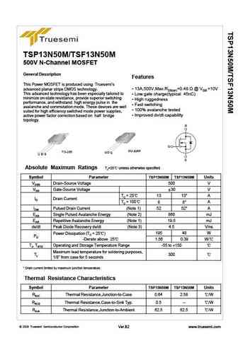
TSP13N50M/TSF13N50M 500V N-Channel MOSFET General Description Features This Power MOSFET is produced using Truesemi s 13A,500V,Max.RDS(on)=0.48 @ VGS =10V advanced planar stripe DMOS technology. This advanced technology has been especially tailored to Low gate charge(typical 45nC) minimize on-state resistance, provide superior switching High ruggedness perfo... See More ⇒
wmm13n50c4 wml13n50c4 wmo13n50c4 wmn13n50c4 wmp13n50c4 wmk13n50c4.pdf
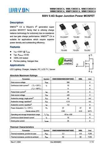
WMM13N50C4, WML13N5 WM C4 50C4, MO13N50C WMN13N50C4, WMP13N5 WM C4 50C4, MK13N50C 500V 0.4 S unction Power M T V Super Ju MOSFET Descrip ption WMOSTM C4 is Wa 4th generation super ayon s n junction MOSFET fa that is utilizing charge M amily S balance te or extremely esistance echnology fo y low on-re D S D G G G S D G and low ga charge performanc WMO... See More ⇒
wmk13n50d1b wml13n50d1b.pdf
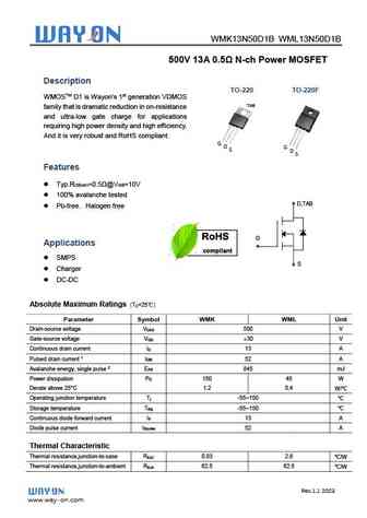
WMK13N50D1B WML13N50D1B 500V 13A 0.5 N-ch Power MOSFET Description TO-220 TO-220F WMOSTM D1 is Wayon s 1st generation VDMOS TAB family that is dramatic reduction in on-resistance and ultra-low gate charge for applications requiring high power density and high efficiency. And it is very robust and RoHS compliant. G D S G D S Features Typ.R =0.5 @V =10V DS(... See More ⇒
cs13n50fa9h.pdf
Silicon N-Channel Power MOSFET R CS13N50F A9H VDSS 500 V General Description ID 13 A CS13N50F A9H, the silicon N-channel Enhanced PD (TC=25 ) 60 W VDMOSFETs, is obtained by the self-aligned planar RDS(ON)Typ 0.34 Technology which reduce the conduction loss, improve switching performance and enhance the avalanche energy. The transistor can be used in variou... See More ⇒
cs13n50fa9r.pdf
Silicon N-Channel Power MOSFET R CS13N50F A9R General Description VDSS 500 V CS13N50F A9R, the silicon N-channel Enhanced ID 13 A PD(TC=25 ) 42 W VDMOSFETs, is obtained by the self-aligned planar Technology RDS(ON)Typ 0.4 which reduce the conduction loss, improve switching performance and enhance the avalanche energy. The transistor can be used in various po... See More ⇒
cs13n50a8h.pdf
Silicon N-Channel Power MOSFET R CS13N50 A8H VDSS 500 V General Description ID 13 A CS13N50 A8H, the silicon N-channel Enhanced PD (TC=25 ) 150 W VDMOSFETs, is obtained by the self-aligned planar Technology RDS(ON)Typ 0.34 which reduce the conduction loss, improve switching performance and enhance the avalanche energy. The transistor can be used in various p... See More ⇒
fir13n50fg.pdf
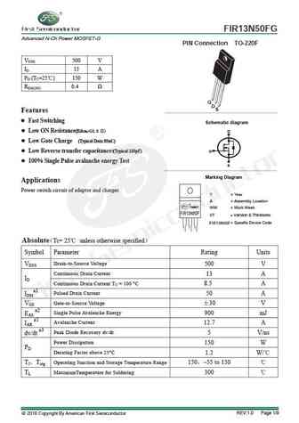
FIR13N50FG CREAT BY ART Advanced N-Ch Power MOSFET-G PIN Connection TO-220F VDSS 500 V ID 13 A PD (TC=25 ) 150 W RDS(ON) 0.4 G D S Features Fast Switching g Schematic dia ram Low ON Resistance(Rdson 0.5 ) D Low Gate Charge (Typical Data 85nC) Low Reverse transfer capacitances(Typical 100pF) G 100% Single Pulse avalanche energy Test S Marking Di... See More ⇒
hfs13n50.pdf
Sep 2009 BVDSS = 500 V RDS(on) typ = 0.4 HFS13N50 ID = 13 A 500V N-Channel MOSFET TO-220F FEATURES 1 Originative New Design 2 3 Superior Avalanche Rugged Technology 1.Gate 2. Drain 3. Source Robust Gate Oxide Technology Very Low Intrinsic Capacitances Excellent Switching Characteristics Unrivalled Gate Charge 38 nC (Typ.) Unrivalled Gate Charge 38 nC (Typ ) Ext... See More ⇒
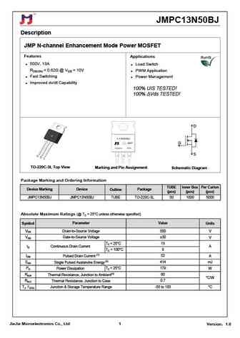
jmpc13n50bj.pdf
JMPC13N50BJ Description JMP N-channel Enhancement Mode Power MOSFET Features Applications 500V, 13A Load Switch RDS(ON) ... See More ⇒
jmpf13n50bj.pdf
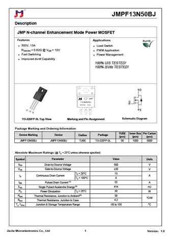
JMPF13N50BJ Description JMP N-channel Enhancement Mode Power MOSFET Features Applications 500V, 13A Load Switch RDS(ON) ... See More ⇒
lnc13n50 lnd13n50.pdf
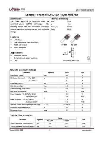
LNC13N50/LND13N50 Lonten N-channel 500V, 13A Power MOSFET Description Product Summary The Power MOSFET is fabricated using the V 500V DSS advanced planar VDMOS technology. The I 13A D resulting device has low conduction resistance, R 0.46 DS(on),max superior switching performance and high avalanche Q 33 nC g,typ energy. Features Low R DS(on) Low gate charge (typ. Q =33 ... See More ⇒
ptf13n50.pdf
PTF1 3 N5 0 5 00V/1 3 A N-Channel A dv anced Power MOSFET Features )@VGS=10V RDS(on) (Typical 0.44 Improved dv/dt Capability, High Ruggedness 100% Avalanche Tested Maximum Junction Temperature Range (150 C) G D S TO-220F Absolute Maximum Ratings Stresses exceeding Maximum Ratings may damage the device. Maximum Ratings are stress ratings only. Functional operation... See More ⇒
smirf13n50.pdf
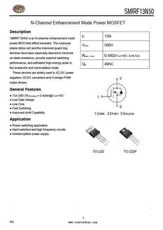
SMIRF13N50 30V /36A Single N Power MOSFET N-Channel Enhancement Mode Power MOSFET Description ID 13A SMIRF13N50 is an N-channel enhancement mode power MOS field effect transistor. The improved VDSS 500V planar stripe cell and the improved guard ring terminal have been especially tailored to minimize Rdson max 0.48 (VGS=10V, ID=6.5A) on-state resistance, provide superi... See More ⇒
vbzm13n50.pdf
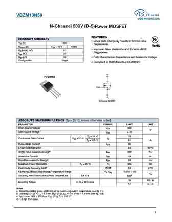
VBZM13N50 www.VBsemi.com N hannel 500 D S Power MOSFET FEATURES PRODUCT SUMMARY Lower Gate Charge Qg Results in Simpler Drive VDS (V) 500 Reqirements RDS(on) ( )VGS = 10 V 0.660 Improved Gate, Avalanche and Dynamic dV/dt Qg (Max.) (nC) 81 Ruggedness Qgs (nC) 20 Qgd (nC) 36 Fully Characterized Capacitance and Avalanche Voltage Configuration Single Complian... See More ⇒
aot13n50.pdf
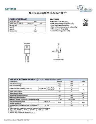
AOT13N50 www.VBsemi.tw N-Channel 650 V (D-S) MOSFET PRODUCT SUMMARY FEATURES VDS (V) at TJ max. 650 Reduced trr, Qrr, and IRRM RDS(on) max. ( ) at 25 C VGS = 10 V 0.34 Low figure-of-merit (FOM) Ron x Qg Qg max. (nC) 106 Low input capacitance (Ciss) Qgs (nC) 14 Low switching losses due to reduced Qrr Ultra low gate charge (Qg) Qgd (nC) 33 Avalanche ener... See More ⇒
vbzmb13n50.pdf
VBZMB13N50 www.VBsemi.com N-Channel (D-S) Power MOSFET 500V FEATURES PRODUCT SUMMARY Lower Gate Charge Qg Results in Simpler Drive VDS (V) 500 Available Reqirements RDS(on) ( )VGS = 10 V 0.80 Improved Gate, Avalanche and Dynamic dV/dt Available Qg (Max.) (nC) 81 Ruggedness Qgs (nC) 20 Qgd (nC) 36 Fully Characterized Capacitance and Avalanche Voltage Configuratio... See More ⇒
hm13n50 hm13n50f.pdf
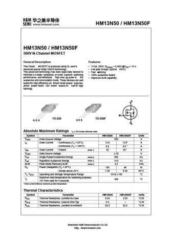
HM13N50 / HM13N50F HM13N50 / HM13N50F 500V N-Channel MOSFET General Description Features This Power MOSFET is produced using SL semi s 13.0A, 500V, RDS(on) = 0.48 @VGS = 10 V advanced planar stripe DMOS technology. Low gate charge ( typical 45nC) This advanced technology has been espe cially tailored to Fast witching s minimize o n-state r esistance, pr ovide superior ... See More ⇒
mp13n50.pdf
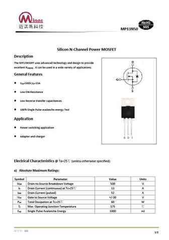
MP13N50 SiliconN-Channel Power MOSFET Description TheMP13N50PF uses advancedtechnology anddesigntoprovide excellent R . It canbeusedinawidevariety of applications. DS(ON) General Features V =500V,I =13A DS D LowONResistance LowReversetransfer capacitances 100%SinglePulseavalancheenergy Test Application Power switchingapplication Adapter andcharger Electrical Characteristics... See More ⇒
mpf13n50.pdf
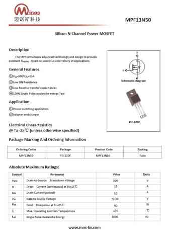
Silicon N-Channel Power MOSFET Description The MPF13N50 uses advanced technology and design to provide excellent RDS(ON) . It can be used in a wide variety of applications. General Features V =500V,I =13A DS D Schematic diagram Low ON Resistance Low Reverse transfer capacitances 100% Single Pulse avalanche energy Test Application Power switching application Adapte... See More ⇒
fxn13n50c.pdf
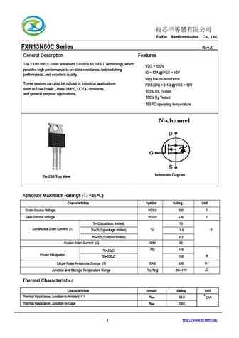
FuXin Semiconductor Co., Ltd. FXN13N50C Series Rev.A General Description Features The FXN13N50C uses advanced Silicon s MOSFET Technology, which VDS = 500V provides high performance in on-state resistance, fast switching ID = 13A @VGS = 10V performance, and excellent quality. Very low on-resistance These devices can also be utilized in indust... See More ⇒
fxn13n50k.pdf
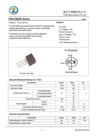
FuXin Semiconductor Co., Ltd. FXN13N50K Series Rev.A General Description Features The FXN13N50K uses advanced Silicon s MOSFET Technology, which V = 500V DS provides high performance in on-state resistance, fast switching ID = 15A @V = 10V GS performance, and excellent quality. Very low on-resistance These devices can also be utilized in industrial a... See More ⇒
mpva13n50f.pdf
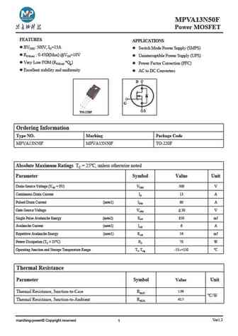
MPVA13N50F Power MOSFET MPSW60M041 FEATURES APPLICATIONS l BVDSS 500V, ID=13A l Switch Mode Power Supply (SMPS) l RDS(on) 0.45 (Max) @VGS=10V l Uninterruptible Power Supply (UPS) l Very Low FOM (RDS(on) *Qg) l Power Factor Correction (PFC) l Excellent stability and uniformity l AC to DC Converters D G S TO-220F Ordering Information Type NO. Marking Package Code MPVA13N5... See More ⇒
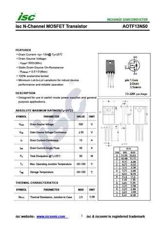
mdp13n50th.pdf
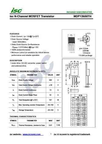
isc N-Channel MOSFET Transistor MDP13N50TH FEATURES Drain Current I = 13A@ T =25 D C Drain Source Voltage V = 500V(Min) DSS Static Drain-Source On-Resistance R = 0.5 (Max) @V = 10V DS(on) GS 100% avalanche tested Minimum Lot-to-Lot variations for robust device performance and reliable operation DESCRIPTION motor drive, DC-DC converter, power switch and solen... See More ⇒
aot13n50.pdf
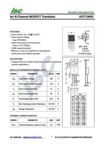
isc N-Channel MOSFET Transistor AOT13N50 FEATURES Drain Current I = 13A@ T =25 D C Drain Source Voltage- V = 500V(Min) DSS Static Drain-Source On-Resistance R = 0.51 (Max) DS(on) 100% avalanche tested Minimum Lot-to-Lot variations for robust device performance and reliable operation DESCRIPTION Designed for use in switch mode power supplies and general purp... See More ⇒
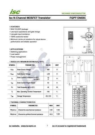
fqpf13n50cf.pdf
isc N-Channel MOSFET Transistor FQPF13N50CF FEATURES Drain Current I =13A@ T =25 D C Drain Source Voltage V =500V(Min) DSS Static Drain-Source On-Resistance R =0.54m (Max) @ V = 10V DS(on) GS 100% avalanche tested Minimum Lot-to-Lot variations for robust device performance and reliable operation DESCRIPTION motor drive, DC-DC converter, power switch and sole... See More ⇒
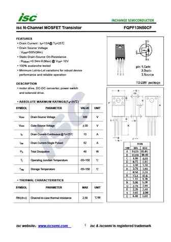
aotf13n50.pdf
isc N-Channel MOSFET Transistor AOTF13N50 FEATURES Drain Current I = 13A@ T =25 D C Drain Source Voltage- V = 500V(Min) DSS Static Drain-Source On-Resistance R = 0.51 (Max) DS(on) 100% avalanche tested Minimum Lot-to-Lot variations for robust device performance and reliable operation DESCRIPTION Designed for use in switch mode power supplies and general pur... See More ⇒
irfb13n50a.pdf
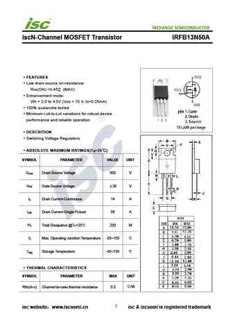
iscN-Channel MOSFET Transistor IRFB13N50A FEATURES Low drain-source on-resistance RDS(ON) =0.45 (MAX) Enhancement mode Vth = 2.0 to 4.0V (VDS = 10 V, ID=0.25mA) 100% avalanche tested Minimum Lot-to-Lot variations for robust device performance and reliable operation DESCRITION Switching Voltage Regulators ABSOLUTE MAXIMUM RATINGS(T =25 ) a SYMBOL PARAMETER VAL... See More ⇒
13n50mf.pdf
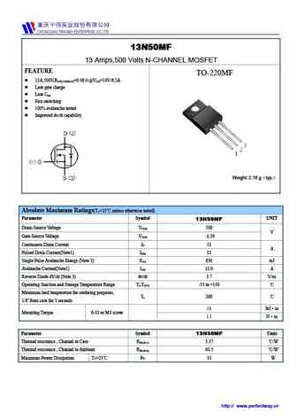
13N50MF 13 Amps,500 Volts N-CHANNEL MOSFET FEATURE TO-220MF 13A,500V,R =0.48 @V =10V/6.5A DS(ON)MAX GS Low gate charge Low C iss Fast switching 100% avalanche tested Improved dv/dt capability Weight 2.16 g typ. Absolute Maximum Ratings(T =25 ,unless otherwise noted) C Parameter Symbol UNIT 13N50MF Drain-Source Voltage V 500 DSS V Gate-Source ... See More ⇒
Detailed specifications: 13N50L-T2Q-T, 13N50G-T2Q-T, 13N50L-TQ2-T, 13N50G-TQ2-T, 13N50L-TQ2-R, 13N50G-TQ2-R, 13N50L-TA3-T, 13N50G-TA3-T, IRF1405, 13N50G-TF3-T, 13N50L-TF1-T, 13N50G-TF1-T, 14N50L-TA3-T, 14N50G-TA3-T, 14N50L-TF1-T, 14N50G-TF1-T, 14N50L-TQ2-T
Keywords - 13N50L-TF3-T MOSFET specs
13N50L-TF3-T cross reference
13N50L-TF3-T equivalent finder
13N50L-TF3-T pdf lookup
13N50L-TF3-T substitution
13N50L-TF3-T replacement
Need a MOSFET replacement? Our guide shows you how to find a perfect substitute by comparing key parameters and specs
🌐 : EN ES РУ

LIST
Last Update
MOSFET: AUW033N08BG | AUW025N10 | AUR030N10 | AUR020N10 | AUR020N085 | AUR014N10 | AUP074N10 | AUP065N10 | AUP062N08BG | AUP060N08AG
Popular searches
2n5401 transistor equivalent | p0903bdg | c1384 transistor | 2sc1175 | 2sc632 | mje15030 transistor equivalent | 13003b | 2n6121