14N50L-TF3-T Specs and Replacement
Type Designator: 14N50L-TF3-T
Type of Transistor: MOSFET
Type of Control Channel: N-Channel
Absolute Maximum Ratings
Pd ⓘ
- Maximum Power Dissipation: 37 W
|Vds|ⓘ - Maximum Drain-Source Voltage: 500 V
|Vgs|ⓘ - Maximum Gate-Source Voltage: 30 V
|Id| ⓘ - Maximum Drain Current: 14 A
Tj ⓘ - Maximum Junction Temperature: 150 °C
Electrical Characteristics
tr ⓘ - Rise Time: 21 nS
Cossⓘ -
Output Capacitance: 170 pF
RDSonⓘ - Maximum Drain-Source On-State Resistance: 0.55 Ohm
Package: TO-220F
14N50L-TF3-T substitution
- MOSFET ⓘ Cross-Reference Search
14N50L-TF3-T datasheet
..1. Size:410K utc
14n50l-tf1-t 14n50g-tf1-t 14n50l-tf3-t 14n50g-tf3-t 14n50l-t3p-t 14n50g-t3p-t.pdf 
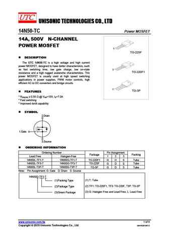
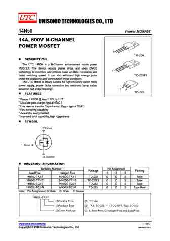
UNISONIC TECHNOLOGIES CO., LTD 14N50-TC Power MOSFET 14A, 500V N-CHANNEL POWER MOSFET 1 TO-220F DESCRIPTION The UTC 14N50-TC is a high voltage and high current power MOSFET, designed to have better characteristics, such as fast switching time, low gate charge, low on-state 1 TO-220F1 resistance and a high rugged avalanche characteristics. This power MOSFET is usually u... See More ⇒
9.2. Size:178K motorola
mtw14n50e.pdf
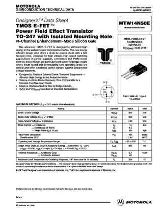
MOTOROLA Order this document SEMICONDUCTOR TECHNICAL DATA by MTW14N50E/D Designer's Data Sheet MTW14N50E TMOS E-FET. Motorola Preferred Device Power Field Effect Transistor TO-247 with Isolated Mounting Hole TMOS POWER FET N Channel Enhancement Mode Silicon Gate 14 AMPERES 500 VOLTS This advanced TMOS E FET is designed to withstand high RDS(on) = 0.40 OHM energy in th... See More ⇒
9.3. Size:205K motorola
mtw14n50erev4.pdf

MOTOROLA Order this document SEMICONDUCTOR TECHNICAL DATA by MTW14N50E/D Designer's Data Sheet MTW14N50E TMOS E-FET. Motorola Preferred Device Power Field Effect Transistor TO-247 with Isolated Mounting Hole TMOS POWER FET N Channel Enhancement Mode Silicon Gate 14 AMPERES 500 VOLTS This advanced TMOS E FET is designed to withstand high RDS(on) = 0.40 OHM energy in th... See More ⇒
9.4. Size:84K philips
phw14n50e 3.pdf
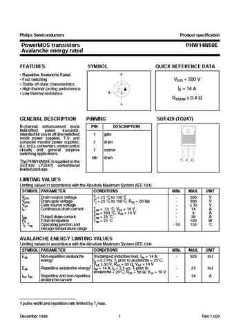
Philips Semiconductors Product specification PowerMOS transistors PHW14N50E Avalanche energy rated FEATURES SYMBOL QUICK REFERENCE DATA d Repetitive Avalanche Rated Fast switching VDSS = 500 V Stable off-state characteristics High thermal cycling performance ID = 14 A g Low thermal resistance RDS(ON) 0.4 s GENERAL DESCRIPTION PINNING SOT429 (TO247) N... See More ⇒
9.6. Size:178K vishay
sihg14n50d.pdf
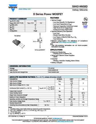
SiHG14N50D www.vishay.com Vishay Siliconix D Series Power MOSFET FEATURES PRODUCT SUMMARY Optimal Design VDS (V) at TJ max. 550 - Low Area Specific On-Resistance RDS(on) max. at 25 C ( ) VGS = 10 V 0.4 - Low Input Capacitance (Ciss) Qg (Max.) (nC) 58 - Reduced Capacitive Switching Losses Qgs (nC) 8 - High Body Diode Ruggedness Qgd (nC) 14 - Avalanche Energy Rated (UIS) ... See More ⇒
9.7. Size:208K vishay
sihp14n50d.pdf
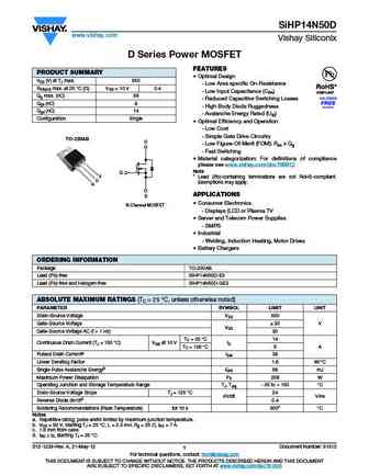
SiHP14N50D www.vishay.com Vishay Siliconix D Series Power MOSFET FEATURES PRODUCT SUMMARY Optimal Design VDS (V) at TJ max. 550 - Low Area specific On-Resistance RDS(on) max. at 25 C ( ) VGS = 10 V 0.4 - Low Input Capacitance (Ciss) Qg max. (nC) 58 - Reduced Capacitive Switching Losses Qgs (nC) 8 - High Body Diode Ruggedness Qgd (nC) 14 - Avalanche Energy Rated (UIS) Co... See More ⇒
9.8. Size:103K onsemi
mtw14n50e.pdf
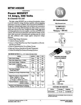
MTW14N50E Preferred Device Power MOSFET 14 Amps, 500 Volts N Channel TO 247 This high voltage MOSFET uses an advanced termination scheme to provide enhanced voltage blocking capability without degrading http //onsemi.com performance over time. In addition, this advanced Power MOSFET is designed to withstand high energy in the avalanche and commutation 14 AMPERES modes. The new ... See More ⇒
9.9. Size:193K utc
14n50.pdf
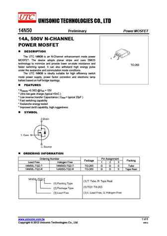
UNISONIC TECHNOLOGIES CO., LTD 14N50 Preliminary Power MOSFET 14A, 500V N-CHANNEL POWER MOSFET DESCRIPTION The UTC 14N50 is an N-Channel enhancement mode power 1 MOSFET. The device adopts planar stripe and uses DMOS technology to minimize and provide lower on-state resistance and TO-263 faster switching speed. It can also withstand high energy pulse under the avalanche and... See More ⇒
9.10. Size:324K aosemi
aowf14n50.pdf
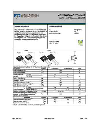
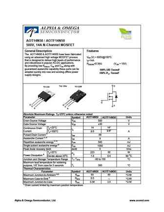
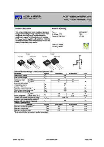
AOW14N50/AOWF14N50 500V, 14A N-Channel MOSFET General Description Product Summary VDS The AOW14N50 & AOWF14N50 have been fabricated 600V@150 using an advanced high voltage MOSFET process that is 14A ID (at VGS=10V) designed to deliver high levels of performance and ... See More ⇒
9.11. Size:258K aosemi
aob14n50.pdf
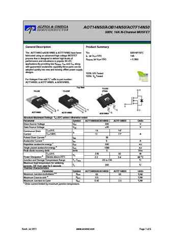
AOT14N50/AOB14N50/AOTF14N50 500V, 14A N-Channel MOSFET General Description Product Summary VDS 600V@150 The AOT14N50 &AOB14N50 & AOTF14N50 have been fabricated using an advanced high voltage MOSFET ID (at VGS=10V) 14A process that is designed to deliver high levels of RDS(ON) (at VGS=10V) ... See More ⇒
9.12. Size:258K aosemi
aot14n50.pdf

AOT14N50/AOB14N50/AOTF14N50 500V, 14A N-Channel MOSFET General Description Product Summary VDS 600V@150 The AOT14N50 &AOB14N50 & AOTF14N50 have been fabricated using an advanced high voltage MOSFET ID (at VGS=10V) 14A process that is designed to deliver high levels of RDS(ON) (at VGS=10V) ... See More ⇒
9.13. Size:232K aosemi
aotf14n50fd.pdf

AOT14N50FD/AOTF14N50FD 500V, 14A N-Channel MOSFET General Description Product Summary VDS 600V@150 The AOT14N50FD/AOTF14N50FD have been fabricated using an advanced high voltage MOSFET process that is ID (at VGS=10V) 14A designed to deliver high levels of performance and RDS(ON) (at VGS=10V) ... See More ⇒
9.14. Size:232K aosemi
aot14n50fd.pdf
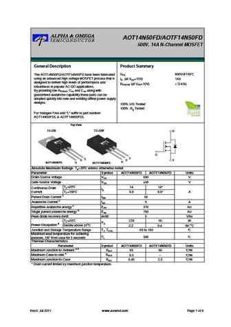
AOT14N50FD/AOTF14N50FD 500V, 14A N-Channel MOSFET General Description Product Summary VDS 600V@150 The AOT14N50FD/AOTF14N50FD have been fabricated using an advanced high voltage MOSFET process that is ID (at VGS=10V) 14A designed to deliver high levels of performance and RDS(ON) (at VGS=10V) ... See More ⇒
9.15. Size:258K aosemi
aotf14n50.pdf

AOT14N50/AOB14N50/AOTF14N50 500V, 14A N-Channel MOSFET General Description Product Summary VDS 600V@150 The AOT14N50 &AOB14N50 & AOTF14N50 have been fabricated using an advanced high voltage MOSFET ID (at VGS=10V) 14A process that is designed to deliver high levels of RDS(ON) (at VGS=10V) ... See More ⇒
9.16. Size:180K aosemi
aot14n50 aotf14n50.pdf
AOT14N50 / AOTF14N50 500V, 14A N-Channel MOSFET General Description Features The AOT14N50 & AOTF14N50 have been fabricated using an advanced high voltage MOSFET process VDS (V) = 600V@150 C that is designed to deliver high levels of performance ID=14A and robustness in popular AC-DC applications. RDS(ON)... See More ⇒
9.17. Size:285K aosemi
aow14n50 aowf14n50.pdf
AOW14N50/AOWF14N50 500V, 14A N-Channel MOSFET General Description Product Summary VDS 600V@150 The AOW14N50 & AOWF14N50 have been fabricated using an advanced high voltage MOSFET process that is ID (at VGS=10V) 14A designed to deliver high levels of performance and RDS(ON) (at VGS=10V) ... See More ⇒
9.18. Size:323K aosemi
aow14n50.pdf

AOW14N50/AOWF14N50 500V, 14A N-Channel MOSFET General Description Product Summary VDS The AOW14N50 & AOWF14N50 have been fabricated 600V@150 using an advanced high voltage MOSFET process that is 14A ID (at VGS=10V) designed to deliver high levels of performance and ... See More ⇒
9.19. Size:123K inpower semi
fta14n50c ftp14n50c.pdf
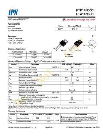
FTP14N50C FTA14N50C N-Channel MOSFET Pb Lead Free Package and Finish Applications VDSS RDS(ON) (Max.) ID Adaptor TV Main Power 500V 0.46 14 A LCD Panel Power D Features RoHS Compliant Low ON Resistance Low Gate Charge G G G Ordering Information DS DS TO-220F TO-220 S PART NUMBER PACKAGE BRAND Packages FTP14N50C TO-220 FTP14N50C Not to Sc... See More ⇒
9.20. Size:190K champion
cmt14n50.pdf
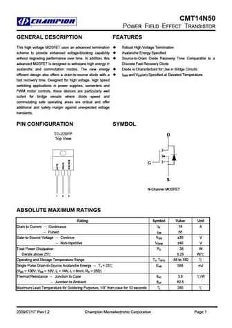
CMT14N50 POWER FIELD EFFECT TRANSISTOR GENERAL DESCRIPTION FEATURES This high voltage MOSFET uses an advanced termination Robust High Voltage Termination scheme to provide enhanced voltage-blocking capability Avalanche Energy Specified without degrading performance over time. In addition, this Source-to-Drain Diode Recovery Time Comparable to a advanced MOSFET is designed to w... See More ⇒
9.21. Size:229K crownpo
ctm14n50.pdf
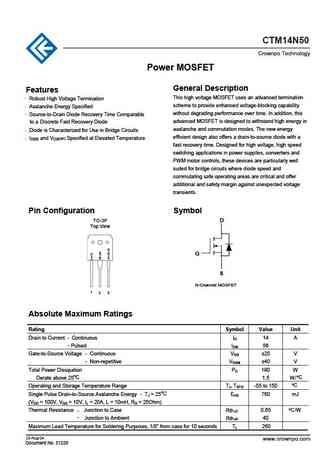
CTM14N50 Crownpo Technology Power MOSFET General Description Features . This high voltage MOSFET uses an advanced termination Robust High Voltage Termination . scheme to provide enhanced voltage-blocking capability Avalanche Energy Specified . without degrading performance over time. In addition, this Source-to-Drain Diode Recovery Time Comparable advanced MOSFET is designed to wit... See More ⇒
9.22. Size:819K samwin
swf14n50d.pdf
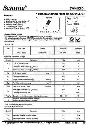
SW14N50D N-channel Enhanced mode TO-220F MOSFET Features TO-220F BVDSS 500V High ruggedness Low RDS(ON) (Typ 0.38 )@VGS=10V ID 14A Low Gate Charge (Typ 54nC) RDS(ON) 0.38 Improved dv/dt Capability 100% Avalanche Tested 2 1 Application Charger, Adaptor, LED 2 3 1 1. Gate 2. Drain 3. Source General Description 3 This power MOSFET is produce... See More ⇒
9.23. Size:4922K first semi
fir14n50fg.pdf
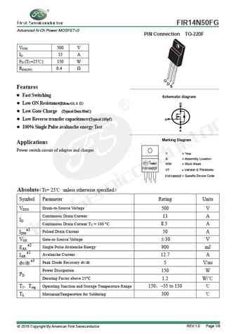
FIR14N50FG CREAT BY ART Advanced N-Ch Power MOSFET-G PIN Connection TO-220F VDSS 500 V ID 13 A PD (TC=25 ) 150 W RDS(ON) 0.4 G D S Features Fast Switching g Schematic dia ram Low ON Resistance(Rdson 0.5 ) D Low Gate Charge (Typical Data 85nC) Low Reverse transfer capacitances(Typical 100pF) G 100% Single Pulse avalanche energy Test S Marking Di... See More ⇒
9.24. Size:253K inchange semiconductor
aob14n50.pdf
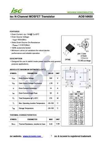
isc N-Channel MOSFET Transistor AOB14N50 FEATURES Drain Current I = 14A@ T =25 D C Drain Source Voltage- V = 500V(Min) DSS Static Drain-Source On-Resistance R = 0.38 (Max) DS(on) 100% avalanche tested Minimum Lot-to-Lot variations for robust device performance and reliable operation DESCRIPTION Designed for use in switch mode power supplies and general purp... See More ⇒
9.25. Size:260K inchange semiconductor
aot14n50.pdf
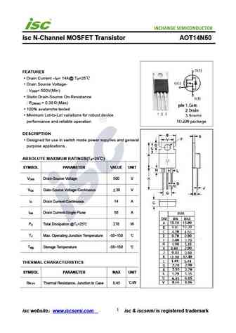
isc N-Channel MOSFET Transistor AOT14N50 FEATURES Drain Current I = 14A@ T =25 D C Drain Source Voltage- V = 500V(Min) DSS Static Drain-Source On-Resistance R = 0.38 (Max) DS(on) 100% avalanche tested Minimum Lot-to-Lot variations for robust device performance and reliable operation DESCRIPTION Designed for use in switch mode power supplies and general purp... See More ⇒
9.26. Size:250K inchange semiconductor
aotf14n50fd.pdf
isc N-Channel MOSFET Transistor AOTF14N50FD FEATURES Drain Current I = 14A@ T =25 D C Drain Source Voltage- V = 500V(Min) DSS Static Drain-Source On-Resistance R = 0.47 (Max) DS(on) 100% avalanche tested Minimum Lot-to-Lot variations for robust device performance and reliable operation DESCRIPTION Designed for use in switch mode power supplies and general p... See More ⇒
9.27. Size:260K inchange semiconductor
aot14n50fd.pdf

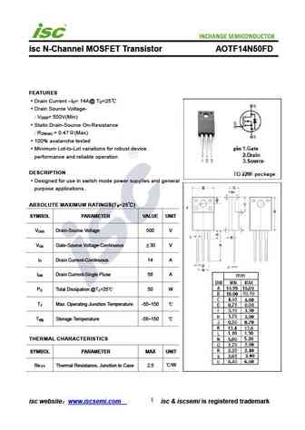
isc N-Channel MOSFET Transistor AOT14N50FD FEATURES Drain Current I = 14A@ T =25 D C Drain Source Voltage- V = 500V(Min) DSS Static Drain-Source On-Resistance R = 0.47 (Max) DS(on) 100% avalanche tested Minimum Lot-to-Lot variations for robust device performance and reliable operation DESCRIPTION Designed for use in switch mode power supplies and general pu... See More ⇒
9.28. Size:250K inchange semiconductor
aotf14n50.pdf
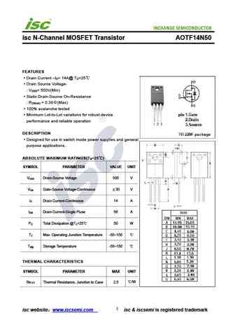
isc N-Channel MOSFET Transistor AOTF14N50 FEATURES Drain Current I = 14A@ T =25 D C Drain Source Voltage- V = 500V(Min) DSS Static Drain-Source On-Resistance R = 0.38 (Max) DS(on) 100% avalanche tested Minimum Lot-to-Lot variations for robust device performance and reliable operation DESCRIPTION Designed for use in switch mode power supplies and general pur... See More ⇒
9.29. Size:298K inchange semiconductor
aow14n50.pdf
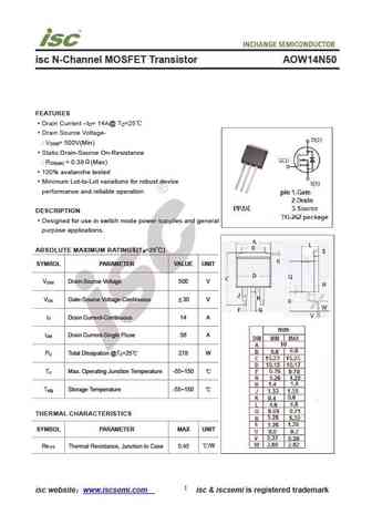
isc N-Channel MOSFET Transistor AOW14N50 FEATURES Drain Current I = 14A@ T =25 D C Drain Source Voltage- V = 500V(Min) DSS Static Drain-Source On-Resistance R = 0.38 (Max) DS(on) 100% avalanche tested Minimum Lot-to-Lot variations for robust device performance and reliable operation DESCRIPTION Designed for use in switch mode power supplies and general purp... See More ⇒
Detailed specifications: 14N50L-TA3-T, 14N50G-TA3-T, 14N50L-TF1-T, 14N50G-TF1-T, 14N50L-TQ2-T, 14N50G-TQ2-T, 14N50L-TQ2-R, 14N50G-TQ2-R, MMIS60R580P, 14N50G-TF3-T, 14N50L-T3P-T, 14N50G-T3P-T, 15N10L-TM3-T, 15N10G-TM3-T, 15N10L-TN3-R, 15N10G-TN3-R, 15N65L-T47-T
Keywords - 14N50L-TF3-T MOSFET specs
14N50L-TF3-T cross reference
14N50L-TF3-T equivalent finder
14N50L-TF3-T pdf lookup
14N50L-TF3-T substitution
14N50L-TF3-T replacement
Need a MOSFET replacement?
Our guide shows you how to find a perfect substitute by comparing key parameters and specs