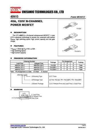
40N15G-TA3-T Specs and Replacement
Type Designator: 40N15G-TA3-T
Type of Transistor: MOSFET
Type of Control Channel: N-Channel
Absolute Maximum Ratings
Pd ⓘ
- Maximum Power Dissipation: 166 W
|Vds|ⓘ - Maximum Drain-Source Voltage: 150 V
|Vgs|ⓘ - Maximum Gate-Source Voltage: 25 V
|Id| ⓘ - Maximum Drain Current: 40 A
Tj ⓘ - Maximum Junction Temperature: 150 °C
Electrical Characteristics
tr ⓘ - Rise Time: 320 nS
Cossⓘ -
Output Capacitance: 520 pF
RDSonⓘ - Maximum Drain-Source On-State Resistance: 0.05 Ohm
Package: TO220
40N15G-TA3-T substitution
- MOSFET ⓘ Cross-Reference Search
40N15G-TA3-T datasheet
9.2. Size:415K samsung
sgl40n150d.pdf 
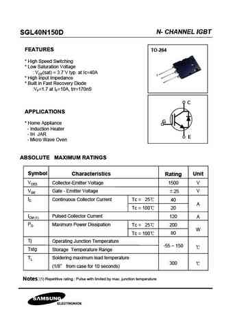
N- CHANNEL IGBT SGL40N150D FEATURES TO-264 * High Speed Switching * Low Saturation Voltage VCE(sat) = 3.7 V typ. at Ic=40A 1 * High Input Impedance * Built in Fast Recovery Diode VF=1.7 at IF=10A, trr=170nS C APPLICATIONS G * Home Appliance - Induction Heater - IH JAR E - Micro Wave Oven ABSOLUTE MAXIMUM RATINGS Symbol Characteristics Unit Rating VCES Collect... See More ⇒
9.3. Size:171K samsung
sgl40n150.pdf
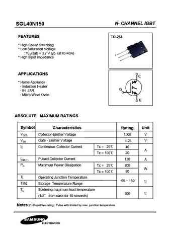
N- CHANNEL IGBT SGL40N150 FEATURES TO-264 * High Speed Switching * Low Saturation Voltage VCE(sat) = 3.7 V typ. (at Ic=40A) 1 * High Input Impedance APPLICATIONS C * Home Appliance - Induction Heater G - IH JAR - Micro Wave Oven E ABSOLUTE MAXIMUM RATINGS Symbol Characteristics Unit Rating VCES Collector-Emitter Voltage V 1500 VGE Gate - Emitter Voltage V 25... See More ⇒
9.4. Size:742K vishay
sqm40n15-38.pdf
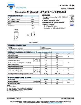
SQM40N15-38 www.vishay.com Vishay Siliconix Automotive N-Channel 150 V (D-S) 175 C MOSFET FEATURES PRODUCT SUMMARY Halogen-free According to IEC 61249-2-21 VDS (V) 150 Definition RDS(on) ( ) at VGS = 10 V 0.038 TrenchFET Power MOSFET RDS(on) ( ) at VGS = 6 V 0.040 Package with Low Thermal Resistance ID (A) 40 AEC-Q101 Qualifiedd Configuration Single 1... See More ⇒
9.5. Size:163K vishay
sum40n15-38.pdf
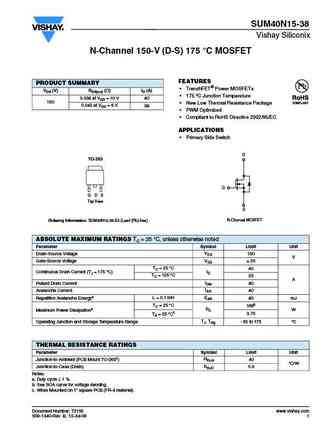
SUM40N15-38 Vishay Siliconix N-Channel 150-V (D-S) 175 C MOSFET FEATURES PRODUCT SUMMARY TrenchFET Power MOSFETs VDS (V) RDS(on) ( )ID (A) 175 C Junction Temperature 0.038 at VGS = 10 V 40 150 New Low Thermal Resistance Package 0.042 at VGS = 6 V 38 PWM Optimized Compliant to RoHS Directive 2002/95/EC APPLICATIONS Primary Side Switch D TO... See More ⇒
9.6. Size:337K ixys
ixtt240n15x4hv ixth240n15x4.pdf
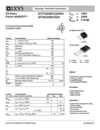
Advance Technical Information X4-Class VDSS = 150V IXTT240N15X4HV Power MOSFETTM ID25 = 240A IXTH240N15X4 RDS(on) 4.4m N-Channel Enhancement Mode Avalanche Rated TO-268HV (IXTT..HV) G Symbol Test Conditions Maximum Ratings S VDSS TJ = 25 C to 175 C 150 V D (Tab) VDGR TJ = 25 C to 175 C, RGS = 1M 150 V TO-247 (IXTH) VGSS Cont... See More ⇒
9.7. Size:658K way-on
wmll040n15hg2.pdf
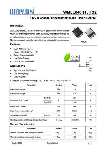
WMLL040N15HG2 150V N-Channel Enhancement Mode Power MOSFET Description D D WMLL040N15HG2 uses Wayon's 2nd generation power trench S MOSFET technology that has been especially tailored to minimize the S G S S S S S S S S on-state resistance and yet maintain superior switching performance. S S G S S This device is well suited for high efficiency fast switching applicat... See More ⇒
9.8. Size:679K way-on
wmm040n15hg2.pdf
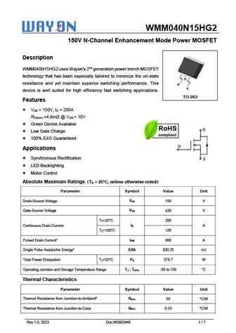
WMM040N15HG2 150V N-Channel Enhancement Mode Power MOSFET Description WMM040N15HG2 uses Wayon's 2nd generation power trench MOSFET technology that has been especially tailored to minimize the on-state D resistance and yet maintain superior switching performance. This G S device is well suited for high efficiency fast switching applications. TO-263 Features V = 150V, I = ... See More ⇒
9.9. Size:4219K first semi
fir40n15lg.pdf
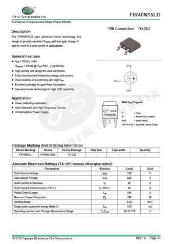
FIR40N15LG N-Channel Enhancement Mode Power Mosfet PIN Connection TO-252 Description The FIR40N15LG uses advanced trench technology and design to provide excellent RDS(ON) with low gate charge. It can be used in a wide variety of applications. General Features VDS =150V,ID =40A RDS(ON) ... See More ⇒
9.10. Size:904K cn hunteck
hgn240n15s.pdf
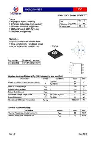
P-1 HGN240N15S 150V N-Ch Power MOSFET Feature 150 V VDS High Speed Power Switching 21 RDS(on),typ VGS=10V mW Enhanced Body diode dv/dt capability 43 A ID (Sillicon Limited) Enhanced Avalanche Ruggedness 100% UIS Tested, 100% Rg Tested Lead Free, Halogen Free Application Synchronous Rectification in SMPS Drain Hard Switching and High Speed Circuit D... See More ⇒
9.11. Size:608K cn hmsemi
hm40n15ka.pdf
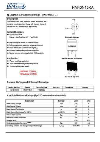
N-Channel Enhancement Mode Power MOSFET Description The uses advanced trench technology and design to provide excellent RDS(ON) with low gate charge. It can be used in a wide variety of applications. General Features VDS =150V,ID =40A RDS(ON) ... See More ⇒
9.12. Size:511K cn hmsemi
hm40n15k.pdf
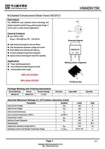
HM40N15K N-Channel Enhancement Mode Power MOSFET Description The HM40N15K uses advanced trench technology and design to provide excellent RDS(ON) with low gate charge. It can be used in a wide variety of applications. General Features VDS =150V,ID =40A RDS(ON) ... See More ⇒
9.13. Size:220K inchange semiconductor
40n15.pdf
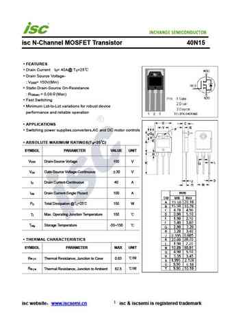
isc N-Channel MOSFET Transistor 40N15 FEATURES Drain Current I = 40A@ T =25 D C Drain Source Voltage- V = 150V(Min) DSS Static Drain-Source On-Resistance R = 0.08 (Max) DS(on) Fast Switching Minimum Lot-to-Lot variations for robust device performance and reliable operation APPLICATIONS Switching power supplies,converters,AC and DC motor controls ABSOLUTE... See More ⇒
Detailed specifications: 3N80G-TF2-T, 3N80L-TM3-T, 3N80G-TM3-T, 3N80L-TMS4-R, 3N80G-TMS4-R, 3N80L-TN3-R, 3N80G-TN3-R, 40N15L-TA3-T, 50N06, 40N15L-TF1-T, 40N15G-TF1-T, 40N15L-TF2-T, 40N15G-TF2-T, 4N100L-TA3-T, 4N100G-TA3-T, 4N100L-TF1-T, 4N100G-TF1-T
Keywords - 40N15G-TA3-T MOSFET specs
40N15G-TA3-T cross reference
40N15G-TA3-T equivalent finder
40N15G-TA3-T pdf lookup
40N15G-TA3-T substitution
40N15G-TA3-T replacement
Step-by-step guide to finding a MOSFET replacement. Cross-reference parts and ensure compatibility for your repair or project.