HY1808AM Specs and Replacement
Type Designator: HY1808AM
Type of Transistor: MOSFET
Type of Control Channel: N-Channel
Absolute Maximum Ratings
Pd ⓘ - Maximum Power Dissipation: 210 W
|Vds|ⓘ - Maximum Drain-Source Voltage: 80 V
|Vgs|ⓘ - Maximum Gate-Source Voltage: 25 V
|Id| ⓘ - Maximum Drain Current: 84 A
Tj ⓘ - Maximum Junction Temperature: 175 °C
Electrical Characteristics
tr ⓘ - Rise Time: 40 nS
Cossⓘ - Output Capacitance: 446 pF
RDSonⓘ - Maximum Drain-Source On-State Resistance: 0.0085 Ohm
Package: TO-220
HY1808AM substitution
- MOSFET ⓘ Cross-Reference Search
HY1808AM datasheet
hy1808ap hy1808m hy1808b hy1808ps hy1808pm.pdf
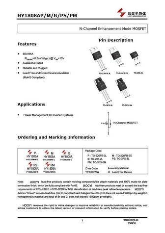
HY1808AP/M/B/PS/PM N-Channel Enhancement Mode MOSFET Pin Description eatures F 80V/84A RDS(ON)=6.2m (typ.) @ VGS=10V S Avalanche Rated D S D G G Reliable and Rugged S D G Lead Free and Green Devices Available TO-263-2L TO-220FB-3L TO-220FB-3S (RoHS Compliant) S D G S D G Applications TO-3PS-3L TO-3PS-3M D Power Management for Inverter Systems. G N-Channe... See More ⇒
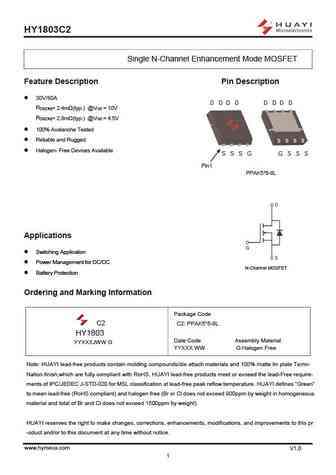
hy1803c2.pdf
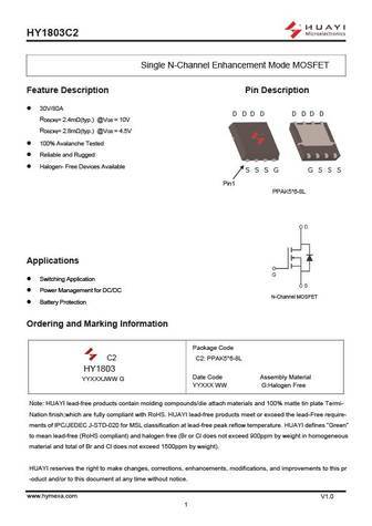
HY1803C2 Single N-Channel Enhancement Mode MOSFET Feature Description Pin Description 30V/80A D D D D D D D D RDS(ON)= 2.4m (typ.) @VGS = 10V RDS(ON)= 2.8m (typ.) @VGS = 4.5V 100% Avalanche Tested Reliable and Rugged Halogen- Free Devices Available S S S G G S S S Pin1 PPAK5*6-8L Applications Switching Application Power Management for DC/DC N-Channel MOSFET ... See More ⇒
hy1804p hy1804b.pdf
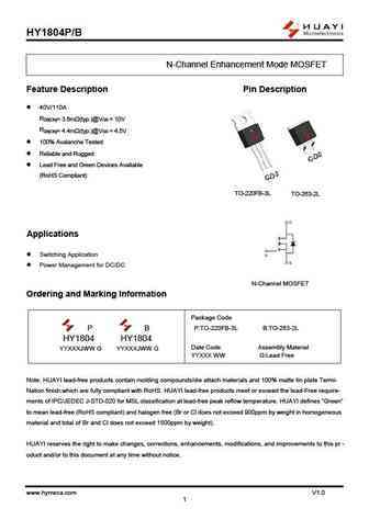
HY1804P/B N-Channel Enhancement Mode MOSFET Feature Description Pin Description 40V/110A RDS(ON)= 3.6m (typ.)@VGS = 10V RDS(ON)= 4.4m (typ.)@VGS = 4.5V 100% Avalanche Tested Reliable and Rugged S GD Lead Free and Green Devices Available (RoHS Compliant) GDS TO-220FB-3L TO-263-2L Applications Switching Application Power Management for DC/DC N-Channel MO... See More ⇒
hy1804d hy1804v.pdf
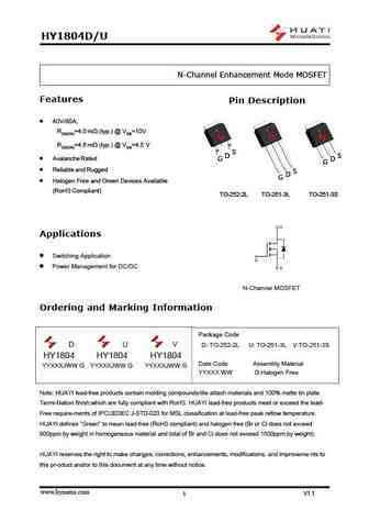
HY1804D/U N-Channel Enhancement Mode MOSFET Features Pin Description 40V/80A, RDS(ON)=4.0 m (typ.) @ VGS=10V RDS(ON)=4.6 m (typ.) @ VGS=4.5 V S S D S D S Avalanche Rated G D G D G G Reliable and Rugged S S D D G Halogen Free and Green Devices Available (RoHS Compliant) TO-252-2L TO-251-3L TO-251-3S Applications Switching Application Pow... See More ⇒
Detailed specifications: SPP100N08S2L-07, SPB100N08S2L-07, CEF02N65D, CEP02N65D, CEB02N65D, HYG055N08NS1P, HYG055N08NS1B, HY1808AP, NCEP15T14, HY1808AB, HY1808APS, HY1808APM, MDP1991, NCE8580, SRC60R090B, AONY36352, HM25P06D
Keywords - HY1808AM MOSFET specs
HY1808AM cross reference
HY1808AM equivalent finder
HY1808AM pdf lookup
HY1808AM substitution
HY1808AM replacement
Learn how to find the right MOSFET substitute. A guide to cross-reference, check specs and replace MOSFETs in your circuits.
History: IRFU420APBF | CJS2019 | BSC079N03SG | FCD600N65S3R0
🌐 : EN ES РУ

LIST
Last Update
MOSFET: AUB034N10 | AUB033N08BG | AUB026N085 | AUA062N08BG | AUA060N08AG | AUA056N08BGL | AUA039N10 | ASW80R290E | ASW65R120EFD | ASW65R110E
Popular searches
skd502t datasheet | svf7n65f | 2sc1419 datasheet | 2n4249 datasheet | tip130 | se9302 transistor | fr5305 datasheet | y2 transistor