HM12N20D Specs and Replacement
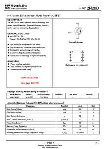
Type Designator: HM12N20D
Type of Transistor: MOSFET
Type of Control Channel: N-Channel
Absolute Maximum Ratings
Pd ⓘ - Maximum Power Dissipation: 150 W
|Vds|ⓘ - Maximum Drain-Source Voltage: 200 V
|Vgs|ⓘ - Maximum Gate-Source Voltage: 20 V
|Id| ⓘ - Maximum Drain Current: 12 A
Tj ⓘ - Maximum Junction Temperature: 175 °C
Electrical Characteristics
tr ⓘ - Rise Time: 18 nS
Cossⓘ - Output Capacitance: 163 pF
RDSonⓘ - Maximum Drain-Source On-State Resistance: 0.08 Ohm
Package: DFN5X6
HM12N20D substitution
- MOSFET ⓘ Cross-Reference Search
HM12N20D datasheet
hm12n20d.pdf
HM N-Channel Enhancement Mode Power MOSFET DESCRIPTION The HM uses advanced trench technology and design to provide excellent RDS(ON) with low gate charge. It can be used in a wide variety of applications. GENERAL FEATURES VDS =200V,ID = A RDS(ON) ... See More ⇒
phm12nq20t.pdf
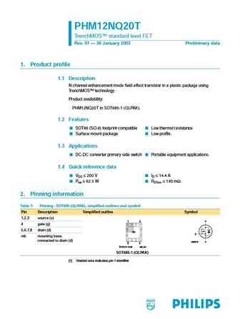
PHM12NQ20T TrenchMOS standard level FET Rev. 01 30 January 2003 Preliminary data 1. Product profile 1.1 Description N-channel enhancement mode field-effect transistor in a plastic package using TrenchMOS technology. Product availability PHM12NQ20T in SOT685-1 (QLPAK). 1.2 Features SOT96 (SO-8) footprint compatible Low thermal resistance Surface mount package Low profile.... See More ⇒
chm12n10pagp.pdf
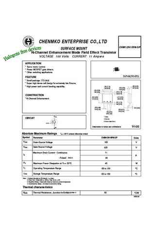
CHENMKO ENTERPRISE CO.,LTD CHM12N10PAGP SURFACE MOUNT N-Channel Enhancement Mode Field Effect Transistor VOLTAGE 100 Volts CURRENT 11 Ampere APPLICATION * Servo motor control. * Power MOSFET gate drivers. * Other switching applications. D-PAK(TO-252) FEATURE * Small package. (TO-252) * Super high dense cell design for extremely low RDS(ON). .094 (2.40) .280 (7.10) * High powe... See More ⇒
Detailed specifications: HM1207E, HM120N03, HM120N03K, HM120N04, HM120N04D, HM120N04I, HM120N04K, HM12N15I, 50N06, HM12N60, HM12N60F, HM12N65, HM12N65F, HM13N50, HM13N50F, HM13P10, HM13P10K
Keywords - HM12N20D MOSFET specs
HM12N20D cross reference
HM12N20D equivalent finder
HM12N20D pdf lookup
HM12N20D substitution
HM12N20D replacement
Step-by-step guide to finding a MOSFET replacement. Cross-reference parts and ensure compatibility for your repair or project.
🌐 : EN ES РУ
LIST
Last Update
MOSFET: AUB062N08BG | AUB060N08AG | AUB056N10 | AUB056N08BGL | AUB050N085 | AUB050N055 | AUB045N12 | AUB045N10BT | AUB039N10 | AUB034N10
Popular searches
кт630 | 2g381 transistor | 2sc2383 transistor equivalent | 2sd669 transistor | 75n65kdf | c2274 transistor | c5200 2sc5200 transistor datasheet | d2390 datasheet
