HM2301A Specs and Replacement
Type Designator: HM2301A
Type of Transistor: MOSFET
Type of Control Channel: P-Channel
Absolute Maximum Ratings
Pd ⓘ
- Maximum Power Dissipation: 1 W
|Vds|ⓘ - Maximum Drain-Source Voltage: 20 V
|Vgs|ⓘ - Maximum Gate-Source Voltage: 12 V
|Id| ⓘ - Maximum Drain Current: 3 A
Tj ⓘ - Maximum Junction Temperature: 150 °C
Electrical Characteristics
tr ⓘ - Rise Time: 35 nS
Cossⓘ -
Output Capacitance: 75 pF
RDSonⓘ - Maximum Drain-Source On-State Resistance: 0.11 Ohm
Package: SOT23
- MOSFET ⓘ Cross-Reference Search
HM2301A datasheet
..1. Size:572K cn hmsemi
hm2301a.pdf 

HM2301A P-Channel Enhancement Mode Power MOSFET DESCRIPTION D The HM2301A uses advanced trench technology to provide excellent RDS(ON), low gate charge and operation with gate G voltages as low as 2.5V. This device is suitable for use as a load switch or in PWM applications. S GENERAL FEATURES Schematic diagram VDS = -20V,ID = -3A RDS(ON) ... See More ⇒
8.1. Size:132K chenmko
chm2301esgp.pdf
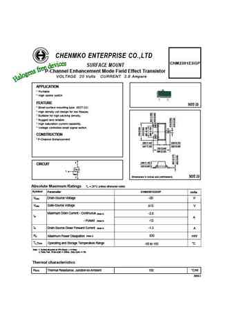
CHENMKO ENTERPRISE CO.,LTD CHM2301ESGP SURFACE MOUNT P-Channel Enhancement Mode Field Effect Transistor VOLTAGE 20 Volts CURRENT 2.8 Ampere APPLICATION * Po rtable * High speed switch FEATURE SOT-23 * Small surface mounting type. (SOT-23) * High density cell design for low RDS(ON) * Suitable for high packing density. * Rugged and reliable. (1) * High saturation current capabili... See More ⇒
8.2. Size:1768K cn vbsemi
hm2301kr.pdf
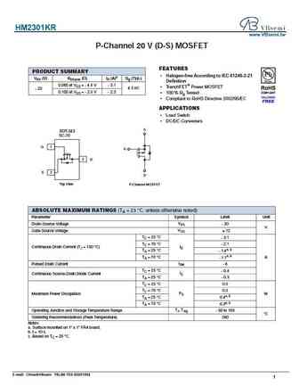
HM2301KR www.VBsemi.tw P-Channel 20 V (D-S) MOSFET FEATURES PRODUCT SUMMARY Halogen-free According to IEC 61249-2-21 VDS (V) RDS(on) ( )ID (A)c Qg (Typ.) Definition 0.080 at VGS = - 4.5 V - 3.1 TrenchFET Power MOSFET 4.3 nC - 20 0.100 at VGS = - 2.5 V - 2.3 100 % Rg Tested Compliant to RoHS Directive 2002/95/EC APPLICATIONS Load Switch DC/DC Convert... See More ⇒
8.3. Size:652K cn hmsemi
hm2301c.pdf

HM2301 P-Channel Trench Power MOSFET General Description The HM2301 uses advanced trench technology to provide excellent R , low gate charge and operation with gate DS(ON) voltages as low as -2.5V. This device is suitable for use as a battery protection or in other switching application. Features Schematic Diagram VDS = -12V,ID =-2. A R ... See More ⇒
8.4. Size:534K cn hmsemi
hm2301.pdf
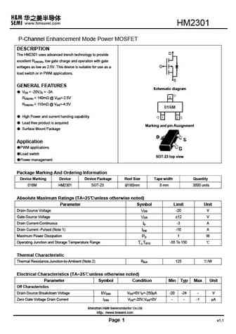
HM2301 P-Channel Enhancement Mode Power MOSFET DESCRIPTION D The HM2301 uses advanced trench technology to provide excellent RDS(ON), low gate charge and operation with gate G voltages as low as 2.5V. This device is suitable for use as a load switch or in PWM applications. S GENERAL FEATURES Schematic diagram VDS = -20V,ID = -3A RDS(ON) ... See More ⇒
8.5. Size:1133K cn hmsemi
hm2301bkr.pdf
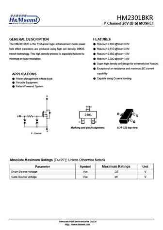
HM2301BKR P-Channel 20V (D-S) MOSFET GENERAL DESCRIPTION FEATURES The HM2301BKR is the P-Channel logic enhancement mode power RDS(ON)= 0.48 @VGS=-4.5V field effect transistors are produced using high cell density, DMOS RDS(ON)= 0.67 @VGS=-2.5V trench technology. This high density process is especially tailored to RDS(ON)= 0.95 @VGS=-1.8V minimize on-state resist... See More ⇒
8.6. Size:1387K cn hmsemi
hm2301bsr.pdf

HM2301BSR P-Channel 20V (D-S) MOSFET GENERAL DESCRIPTION FEATURES The HM2301BSR is the P-Channel logic enhancement mode power RDS(ON)= 0.48 @VGS=-4.5V field effect transistors are produced using high cell density, DMOS RDS(ON)= 0.67 @VGS=-2.5V trench technology. This high density process is especially tailored to RDS(ON)= 0.95 @VGS=-1.8V minimize on-state resist... See More ⇒
8.7. Size:803K cn hmsemi
hm2301b.pdf
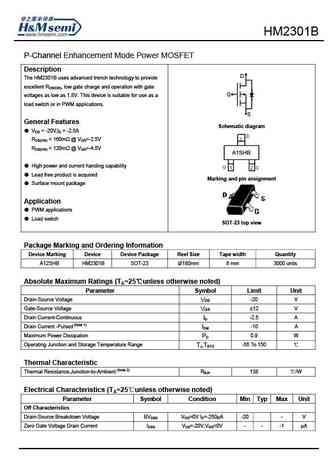
HM2301B P-Channel Enhancement Mode Power MOSFET Description D The HM2301B uses advanced trench technology to provide excellent RDS(ON), low gate charge and operation with gate G voltages as low as 1.8V. This device is suitable for use as a load switch or in PWM applications. S General Features Schematic diagram VDS = -20V,ID = -2.5A RDS(ON) ... See More ⇒
8.8. Size:727K cn hmsemi
hm2301e.pdf
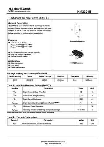
HM2301E P-Channel Trench Power MOSFET General Description The HM2301E uses advanced trench technology to provide excellent R , low gate charge and operation with gate DS(ON) voltages as low as -2.5V. This device is suitable for use as a battery protection or in other switching application. Features Schematic Diagram VDS = -12V,ID =-2.0A R ... See More ⇒
8.9. Size:273K cn hmsemi
hm2301bjr.pdf
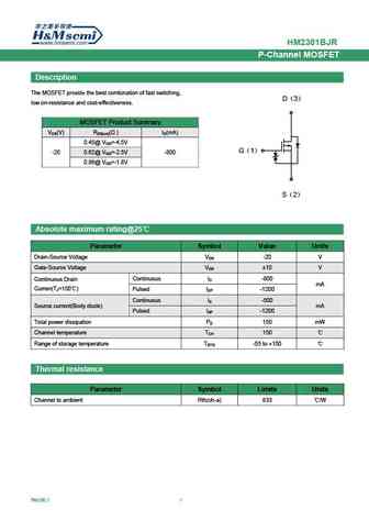
HM2301BJR P-Channel MOSFET Description The MOSFET provide the best combination of fast switching, D 3 low on-resistance and cost-effectiveness. MOSFET Product Summary V (V) R ( ) I (mA) DS DS(on) D 0.45@ V =-4.5V GS G 1 -20 0.62@ VGS=-2.5V -800 0.86@ V =-1.8V GS S 2 Absolute maximum rating@25 Parameter Symbol Value Units Drain-Source Voltage ... See More ⇒
8.10. Size:608K cn hmsemi
hm2301dr.pdf
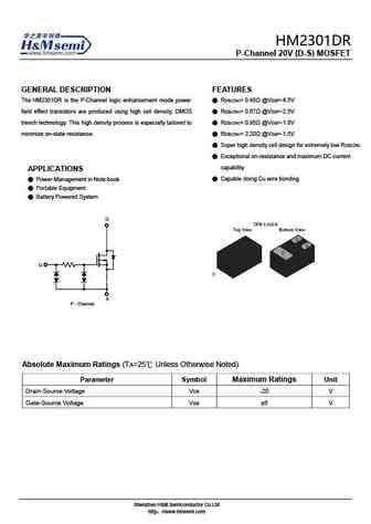
H P-Channel 20V (D-S) MOSFET GENERAL DESCRIPTION FEATURES The is the P-Channel logic enhancement mode power RDS(ON)= 0.48 @VGS=-4.5V field effect transistors are produced using high cell density, DMOS RDS(ON)= 0.67 @VGS=-2.5V trench technology. This high density process is especially tailored to RDS(ON)= 0.95 @VGS=-1.8V minimize on-state resistan... See More ⇒
8.11. Size:704K cn hmsemi
hm2301d.pdf
H P-Channel 20V (D-S) MOSFET GENERAL DESCRIPTION FEATURES The is the P-Channel logic enhancement mode power RDS(ON)= 0.48 @VGS=-4.5V field effect transistors are produced using high cell density, DMOS RDS(ON)= 0.67 @VGS=-2.5V trench technology. This high density process is especially tailored to RDS(ON)= 0.95 @VGS=-1.8V minimize on-state resistance... See More ⇒
8.12. Size:1451K cn hmsemi
hm2301kr.pdf
HM2301KR P-Channel Enhancement Mode Power MOSFET DESCRIPTION D The HM2301KR uses advanced trench technology to provide excellent RDS(ON), low gate charge and operation with gate G voltages as low as 2.5V. This device is suitable for use as a load switch or in PWM applications. S GENERAL FEATURES Schematic diagram VDS = -20V,ID = -3A RDS(ON) ... See More ⇒
8.13. Size:977K cn hmsemi
hm2301f.pdf
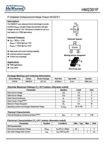
HM2301F P-Channel Enhancement Mode Power MOSFET Description D The HM2301F uses advanced trench technology to provide excellent RDS(ON), low gate charge and operation with gate G voltages as low as 1.8V. This device is suitable for use as a load switch or in PWM applications. S General Features Schematic diagram VDS = -20V,ID = -2.8A RDS(ON) ... See More ⇒
Detailed specifications: HM20P02Q, HM20PD05, HM2300B, HM2300C, HM2300D, HM2300DR, HM2300PR, HM2301, IRFZ46N, HM2301B, HM2301BJR, HM2301BKR, HM2301BSR, HM2301C, HM2301D, HM2301DR, HM2301E
Keywords - HM2301A MOSFET specs
HM2301A cross reference
HM2301A equivalent finder
HM2301A pdf lookup
HM2301A substitution
HM2301A replacement
Learn how to find the right MOSFET substitute. A guide to cross-reference, check specs and replace MOSFETs in your circuits.
