HM2302 Specs and Replacement
Type Designator: HM2302
Type of Transistor: MOSFET
Type of Control Channel: N-Channel
Absolute Maximum Ratings
Pd ⓘ - Maximum Power Dissipation: 1 W
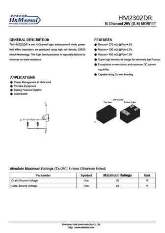
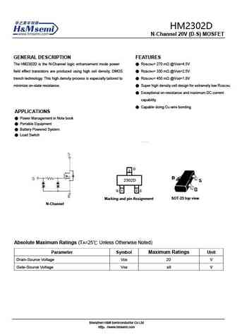
|Vds|ⓘ - Maximum Drain-Source Voltage: 20 V
|Vgs|ⓘ - Maximum Gate-Source Voltage: 10 V
|Id| ⓘ - Maximum Drain Current: 2.9 A
Tj ⓘ - Maximum Junction Temperature: 150 °C
Electrical Characteristics
tr ⓘ - Rise Time: 50 nS
Cossⓘ - Output Capacitance: 120 pF
RDSonⓘ - Maximum Drain-Source On-State Resistance: 0.045 Ohm
Package: SOT23
HM2302 substitution
- MOSFET ⓘ Cross-Reference Search
HM2302 datasheet
hm2302.pdf

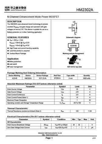
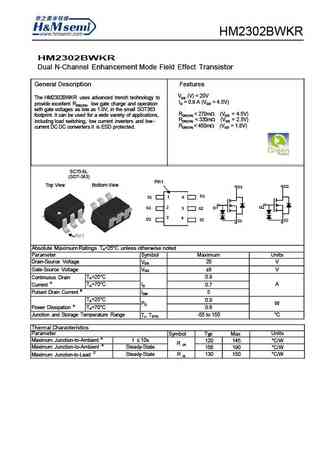
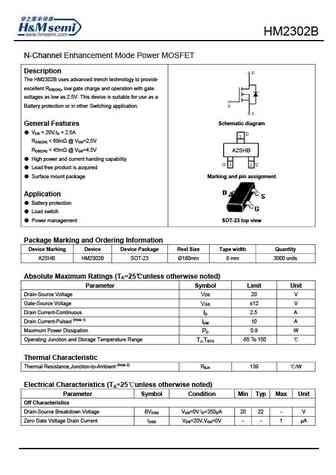
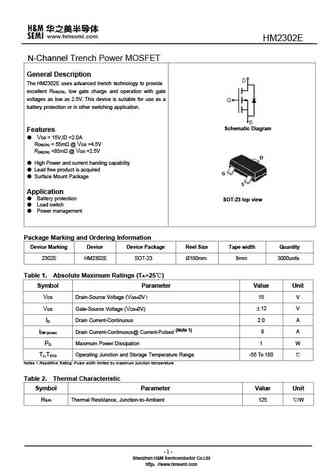
HM2302 N-Channel Enhancement Mode Power MOSFET DESCRIPTION D The HM2302 uses advanced trench technology to provide excellent RDS(ON), low gate charge and operation with gate G voltages as low as 2.5V. This device is suitable for use as a Battery protection or in other Switching application. S Schematic diagram GENERAL FEATURES VDS = 20V,ID = 2.9A D 3 RDS(ON) ... See More ⇒
hm2302bwsr.pdf
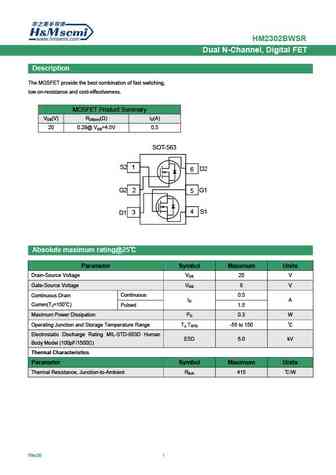
Description The MOSFET provide the best combination of fast switching, low on-resistance and cost-effectiveness. MOSFET Product Summary VDS(V) RDS(on)( ) ID(A) 20 0.29@ VGS=4.5V 0.5 SOT-563 S2 1 D2 6 G2 2 G1 5 4 S1 3 D1 Absolute maximum rating@25 Parameter Symbol Maximum Units Drain-Source Voltage ... See More ⇒
hm2302kr.pdf
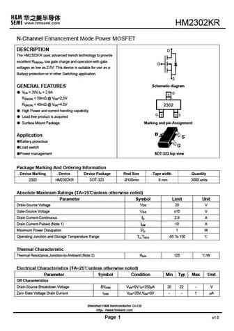
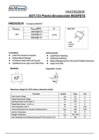
HM2302KR N-Channel Enhancement Mode Power MOSFET DESCRIPTION D The HM2302KR uses advanced trench technology to provide excellent RDS(ON), low gate charge and operation with gate G voltages as low as 2.5V. This device is suitable for use as a Battery protection or in other Switching application. S Schematic diagram GENERAL FEATURES VDS = 20V,ID = 2.9A D 3 RDS(ON) ... See More ⇒
hm2302f.pdf

HM2302F N-Channel Enhancement Mode Power MOSFET Description The HM2302F uses advanced trench technology to provide excellent RDS(ON), low gate charge and operation with gate voltages as low as 2.5V. This device is suitable for use as a Battery protection or in other Switching application. Schematic diagram General Features VDS = 20V,ID = 2.8A RDS(ON) ... See More ⇒
Detailed specifications: HM2301BJR, HM2301BKR, HM2301BSR, HM2301C, HM2301D, HM2301DR, HM2301E, HM2301F, AOD4184A, HM2302A, HM2302B, HM2302BJR, HM2302BWKR, HM2302BWSR, HM2302D, HM2302DR, HM2302E
Keywords - HM2302 MOSFET specs
HM2302 cross reference
HM2302 equivalent finder
HM2302 pdf lookup
HM2302 substitution
HM2302 replacement
Can't find your MOSFET? Learn how to find a substitute transistor by analyzing voltage, current and package compatibility
History: AOI4T60P | AS2341
🌐 : EN ES РУ

LIST
Last Update
MOSFET: AUN084N10 | AUN065N10 | AUN063N10 | AUN062N08BG | AUN060N08AG | AUN053N10 | AUN050N08BGL | AUN045N085 | AUN042N055 | AUN036N10
Popular searches
bc547 datasheet | k3797 mosfet | bs170 datasheet | tip41c | irfp460 | irfz44n mosfet | lm317t datasheet | irf540