HM2314 Specs and Replacement
Type Designator: HM2314
Type of Transistor: MOSFET
Type of Control Channel: N-Channel
Absolute Maximum Ratings
Pd ⓘ
- Maximum Power Dissipation: 1.25 W
|Vds|ⓘ - Maximum Drain-Source Voltage: 20 V
|Vgs|ⓘ - Maximum Gate-Source Voltage: 12 V
|Id| ⓘ - Maximum Drain Current: 4.5 A
Tj ⓘ - Maximum Junction Temperature: 150 °C
Electrical Characteristics
tr ⓘ - Rise Time: 18 nS
Cossⓘ -
Output Capacitance: 300 pF
RDSonⓘ - Maximum Drain-Source On-State Resistance: 0.033 Ohm
Package: SOT23
- MOSFET ⓘ Cross-Reference Search
HM2314 datasheet
..1. Size:555K cn hmsemi
hm2314.pdf 

HM2314 N-Channel Enhancement Mode Power MOSFET Description D The HM2314 uses advanced trench technology to provide excellent RDS(ON), low gate charge and operation with gate G voltages as low as 2.5V. This device is suitable for use as a battery protection or in other switching application. S Schematic diagram General Features VDS = 20V,ID = 4.5A RDS(ON) ... See More ⇒
0.1. Size:74K chenmko
chm2314gp.pdf
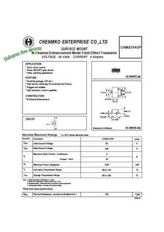
CHENMKO ENTERPRISE CO.,LTD CHM2314GP SURFACE MOUNT N-Channel Enhancement Mode Field Effect Transistor VOLTAGE 30 Volts CURRENT 4 Ampere APPLICATION * Servo motor control. * Power MOSFET gate drivers. * Other switching applications. SC-59/SOT-346 FEATURE * Small flat package. (SC-59 ) * High density cell design for extremely low RDS(ON). * Rugged and reliable. (2) * High satur... See More ⇒
0.2. Size:711K cn hmsemi
hm2314b.pdf
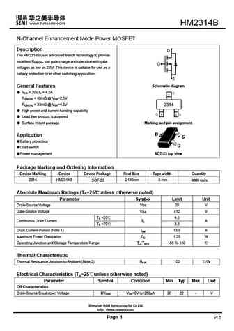
HM2314B N-Channel Enhancement Mode Power MOSFET Description D The HM2314B uses advanced trench technology to provide excellent RDS(ON), low gate charge and operation with gate G voltages as low as 2.5V. This device is suitable for use as a battery protection or in other switching application. S Schematic diagram General Features VDS = 20V,ID = 4.5A RDS(ON) ... See More ⇒
9.1. Size:413K chenmko
chm2313qgp.pdf
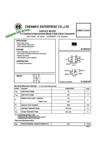
CHENMKO ENTERPRISE CO.,LTD CHM2313QGP SURFACE MOUNT P-Channel Enhancement Mode Field Effect Transistor VOLTAGE 30 Volts CURRENT 4.6 Ampere APPLICATION * Servo motor control. * Power MOSFET gate drivers. * Other switching applications. SC-74/SOT-457 FEATURE * Small flat package. (SC-74/SOT-457) * High density cell design for extremely low RDS(ON). * Rugged and reliable. (1) (6) ... See More ⇒
9.2. Size:69K chenmko
chm2316gp.pdf
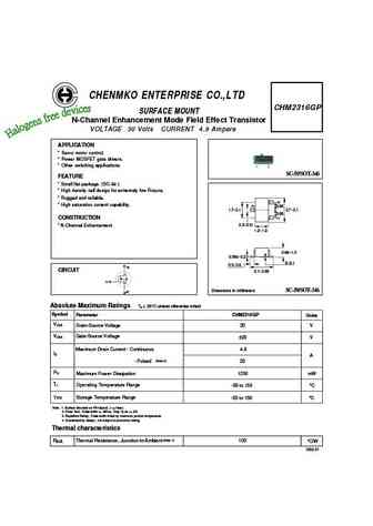
CHENMKO ENTERPRISE CO.,LTD CHM2316GP SURFACE MOUNT N-Channel Enhancement Mode Field Effect Transistor VOLTAGE 30 Volts CURRENT 4.8 Ampere APPLICATION * Servo motor control. * Power MOSFET gate drivers. * Other switching applications. SC-59/SOT-346 FEATURE * Small flat package. (SC-59 ) * High density cell design for extremely low RDS(ON). * Rugged and reliable. (2) * High sat... See More ⇒
9.3. Size:108K chenmko
chm2316qgp.pdf
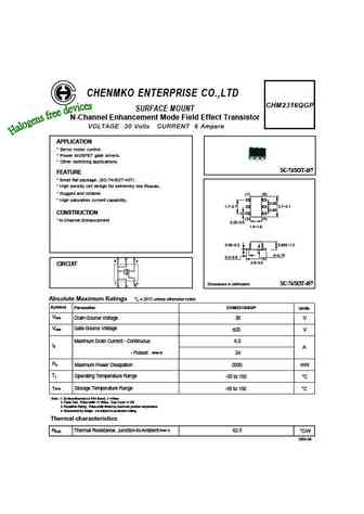
CHENMKO ENTERPRISE CO.,LTD CHM2316QGP SURFACE MOUNT N-Channel Enhancement Mode Field Effect Transistor VOLTAGE 30 Volts CURRENT 6 Ampere APPLICATION * Servo motor control. * Power MOSFET gate drivers. * Other switching applications. SC-74/SOT-457 FEATURE * Small flat package. (SC-74/SOT-457) * High density cell design for extremely low RDS(ON). * Rugged and reliable. (1) (6) *... See More ⇒
9.4. Size:352K chenmko
chm2310gp.pdf
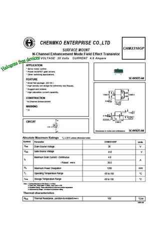
CHENMKO ENTERPRISE CO.,LTD CHM2310GP SURFACE MOUNT N-Channel Enhancement Mode Field Effect Transistor VOLTAGE 30 Volts CURRENT 4.8 Ampere APPLICATION * Servo motor control. * Power MOSFET gate drivers. * Other switching applications. SC-59/SOT-346 FEATURE * Small flat package. (SC-59 ) * High density cell design for extremely low RDS(ON). * Rugged and reliable. * High saturati... See More ⇒
9.5. Size:90K chenmko
chm2313gp.pdf
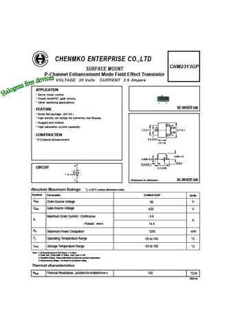
CHENMKO ENTERPRISE CO.,LTD CHM2313GP SURFACE MOUNT P-Channel Enhancement Mode Field Effect Transistor VOLTAGE 30 Volts CURRENT 3.6 Ampere APPLICATION * Servo motor control. * Power MOSFET gate drivers. * Other switching applications. SC-59/SOT-346 FEATURE * Small flat package. (SC-59 ) * High density cell design for extremely low RDS(ON). * Rugged and reliable. (2) * High sat... See More ⇒
9.6. Size:154K chenmko
chm2313gp-a.pdf
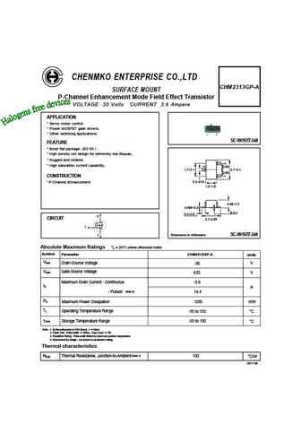
CHENMKO ENTERPRISE CO.,LTD CHM2313GP-A SURFACE MOUNT P-Channel Enhancement Mode Field Effect Transistor VOLTAGE 30 Volts CURRENT 3.6 Ampere APPLICATION * Servo motor control. * Power MOSFET gate drivers. * Other switching applications. SC-59/SOT-346 FEATURE * Small flat package. (SC-59 ) * High density cell design for extremely low RDS(ON). * Rugged and reliable. (2) * High s... See More ⇒
9.7. Size:1675K cn vbsemi
hm2310pr.pdf
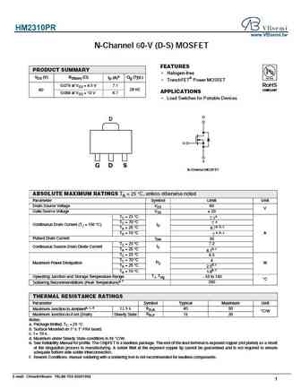
HM2310PR www.VBsemi.tw N-Channel 60-V (D-S) MOSFET FEATURES PRODUCT SUMMARY Halogen-free VDS (V) RDS(on) ( ) ID (A)a Qg (Typ.) TrenchFET Power MOSFET 0.076 at VGS = 4.5 V 7.1 RoHS 29 nC COMPLIANT 60 APPLICATIONS 0.088 at VGS = 10 V 6.7 Load Switches for Portable Devices D D G S G D S N-Channel MOSFET ABSOLUTE MAXIMUM RATINGS TA = 25 C, unless otherwise n... See More ⇒
9.8. Size:1881K cn vbsemi
hm2310.pdf
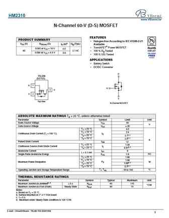
HM2310 www.VBsemi.tw N-Channel 60-V (D-S) MOSFET FEATURES PRODUCT SUMMARY Halogen-free According to IEC 61249-2-21 VDS (V) RDS(on) ( ) ID (A)a Qg (Typ.) Available TrenchFET Power MOSFET 0.085 at VGS = 10 V 4.0 60 2.1 nC 100 % Rg Tested 0.096 at VGS = 4.5 V 3.8 100 % UIS Tested APPLICATIONS Battery Switch DC/DC Converter D TO-236 (SOT23) G 1 ... See More ⇒
9.9. Size:723K cn hmsemi
hm2310b.pdf

HM2310B N Channel Enhancement Mode MOSFET DESCRIPTION The HM2310B is the N-Channel logic enhancement mode power field effect transistor is produced using high cell density, DMOS trench technology. This high-density process is especially tailored to minimize on-state resistance. These devices are particularly suited for low voltage application such as cellular phone and notebook co... See More ⇒
9.10. Size:648K cn hmsemi
hm2312b.pdf

HM2312B N-Channel Enhancement Mode Power MOSFET Description D The HM2312B uses advanced trench technology to provide excellent RDS(ON), low gate charge and operation with gate G voltages as low as 2.5V. This device is suitable for use as a battery protection or in other switching application. S Schematic diagram General Features VDS = 20V,ID = 4.5A RDS(ON) ... See More ⇒
9.11. Size:402K cn hmsemi
hm2318b.pdf
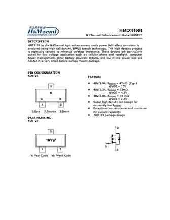
HM2318B N Channel Enhancement Mode MOSFET DESCRIPTION HM2318B is the N-Channel logic enhancement mode power field effect transistor is produced using high cell density, DMOS trench technology. This high density process is especially tailored to minimize on-state resistance. These devices are particularly suited for low voltage application such as cellular phone and notebook computer... See More ⇒
9.12. Size:576K cn hmsemi
hm2310pr.pdf
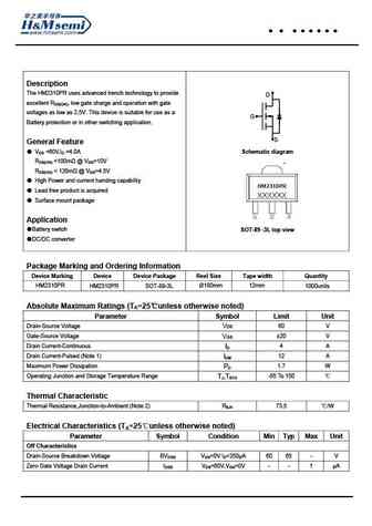
HM2310PR Description The HM2310PR uses advanced trench technology to provide D excellent RDS(ON), low gate charge and operation with gate voltages as low as 2.5V. This device is suitable for use as a G Battery protection or in other switching application. S General Feature VDS =60V,ID =4.0A Schematic diagram RDS(ON) ... See More ⇒
9.13. Size:514K cn hmsemi
hm2319a.pdf
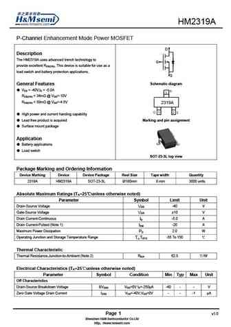
HM2319A P-Channel Enhancement Mode Power MOSFET D Description The HM2319A uses advanced trench technology to G provide excellent RDS(ON), This device is suitable for use as a load switch and battery protection applications. S Schematic diagram General Features VDS = -40V,ID = -5.0A RDS(ON) ... See More ⇒
9.14. Size:476K cn hmsemi
hm2310.pdf
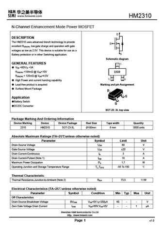
HM2310 N-Channel Enhancement Mode Power MOSFET D DESCRIPTION The HM2310 uses advanced trench technology to provide G excellent RDS(ON), low gate charge and operation with gate voltages as low as 2.5V. This device is suitable for use as a S Battery protection or in other Switching application. Schematic diagram GENERAL FEATURES VDS =60V,ID =3A RDS(ON) ... See More ⇒
9.15. Size:554K cn hmsemi
hm2312.pdf

HM2312 N-Channel Enhancement Mode Power MOSFET Description D The HM2312 uses advanced trench technology to provide excellent RDS(ON), low gate charge and operation with gate G voltages as low as 2.5V. This device is suitable for use as a battery protection or in other switching application. S Schematic diagram General Features VDS = 20V,ID = 4.5A RDS(ON) ... See More ⇒
9.16. Size:1351K cn hmsemi
hm2318apr.pdf
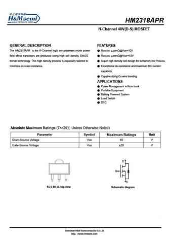
HM2318 N-Channel 40V(D-S) MOSFET GENERAL DESCRIPTION FEATURES The HM is the N-Channel logic enhancement mode power RDS(ON) 28m @VGS=10V field effect transistors are produced using high cell density, DMOS RDS(ON) 38m @VGS=4.5V trench technology. This high density process is especially tailored to Super high density cell design for extremely low RDS(ON) ... See More ⇒
9.17. Size:1187K cn hmsemi
hm2318a.pdf
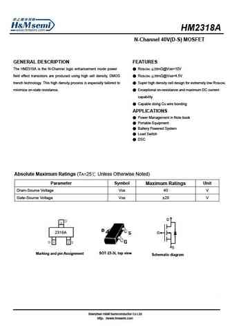
HM2318A N-Channel 40V(D-S) MOSFET GENERAL DESCRIPTION FEATURES The HM2318A is the N-Channel logic enhancement mode power RDS(ON) 28m @VGS=10V field effect transistors are produced using high cell density, DMOS RDS(ON) 38m @VGS=4.5V trench technology. This high density process is especially tailored to Super high density cell design for extremely low RDS(ON) min... See More ⇒
9.18. Size:445K cn hmsemi
hm2319.pdf
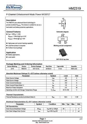
HM2319 P-Channel Enhancement Mode Power MOSFET D Description The HM2319 uses advanced trench technology to G provide excellent RDS(ON), This device is suitable for use as a load switch and battery protection applications. S Schematic diagram General Features VDS = -40V,ID = - A RDS(ON) ... See More ⇒
9.19. Size:719K cn hmsemi
hm2310c.pdf
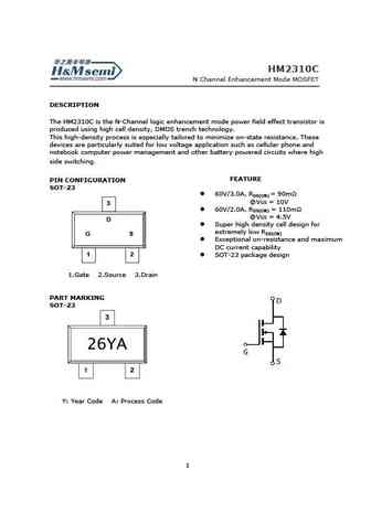
HM N Channel Enhancement Mode MOSFET DESCRIPTION The HM2310C is the N-Channel logic enhancement mode power field effect transistor is produced using high cell density, DMOS trench technology. This high-density process is especially tailored to minimize on-state resistance. These devices are particularly suited for low voltage application such as cellular phone and notebook co... See More ⇒
Detailed specifications: HM2309B, HM2309C, HM2309D, HM2309DR, HM2310B, HM2310C, HM2312, HM2312B, AON6414A, HM2314B, HM2318A, HM2318APR, HM2318B, HM2319, HM2319A, HM2328, HM2333
Keywords - HM2314 MOSFET specs
HM2314 cross reference
HM2314 equivalent finder
HM2314 pdf lookup
HM2314 substitution
HM2314 replacement
Learn how to find the right MOSFET substitute. A guide to cross-reference, check specs and replace MOSFETs in your circuits.
