HM30P55K Specs and Replacement
Type Designator: HM30P55K
Type of Transistor: MOSFET
Type of Control Channel: P-Channel
Absolute Maximum Ratings
Pd ⓘ - Maximum Power Dissipation: 90 W
|Vds|ⓘ - Maximum Drain-Source Voltage: 55 V
|Vgs|ⓘ - Maximum Gate-Source Voltage: 20 V
|Id| ⓘ - Maximum Drain Current: 30 A
Tj ⓘ - Maximum Junction Temperature: 150 °C
Electrical Characteristics
tr ⓘ - Rise Time: 15 nS
Cossⓘ - Output Capacitance: 240 pF
RDSonⓘ - Maximum Drain-Source On-State Resistance: 0.04 Ohm
Package: TO252
HM30P55K substitution
- MOSFET ⓘ Cross-Reference Search
HM30P55K datasheet
hm30p55k.pdf
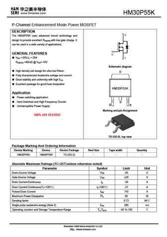
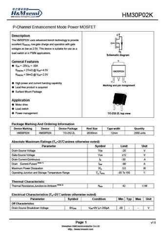
P-Channel Enhancement Mode Power MOSFET DESCRIPTION The uses advanced trench technology and design to provide excellent RDS(ON) with low gate charge. It can be used in a wide variety of applications. GENERAL FEATURES VDS =-55V,ID =-30A RDS(ON) ... See More ⇒
hm30p55.pdf
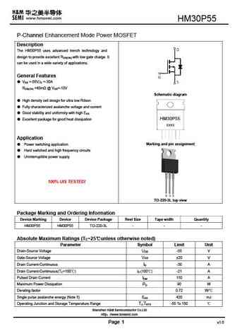
P-Channel Enhancement Mode Power MOSFET Description The uses advanced trench technology and design to provide excellent RDS(ON) with low gate charge. It can be used in a wide variety of applications. General Features VDS =-55V,ID =-30A RDS(ON) ... See More ⇒
hm30p10k.pdf
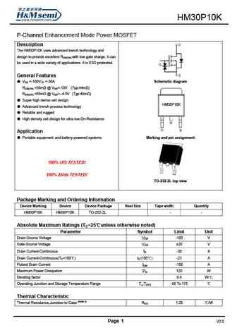
P-Channel Enhancement Mode Power MOSFET Description The uses advanced trench technology and design to provide excellent RDS(ON) with low gate charge. It can be used in a wide variety of applications. It is ESD protested. General Features VDS =-100V,ID =-30A Schematic diagram RDS(ON) ... See More ⇒
hm30p03q.pdf
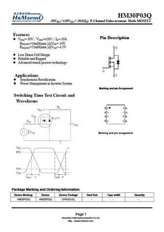
HM30P03Q -30VDS 20VGS -30A(ID) P-Channel Enha ncement Mode MOSFET Features Pin Description Pin Description VDSS=-30V VGSS= 20V ID=-30A RDS(ON)=14m (max.)@VGS=-10V RDS(ON)=22m (max.)@VGS=-4.5V Low Dense Cell Design Reliable and Rugged Advanced trench process technology Applications Synchronous Rectification Power Management in Inverter ... See More ⇒
Detailed specifications: HM30N04Q, HM30N10, HM30N10D, HM30N10K, HM30P02K, HM30P03Q, HM30P10K, HM30P55, EMB04N03H, HM3205, HM3205B, HM3205D, HM3207, HM3207B, HM3207BD, HM3207D, HM3207T
Keywords - HM30P55K MOSFET specs
HM30P55K cross reference
HM30P55K equivalent finder
HM30P55K pdf lookup
HM30P55K substitution
HM30P55K replacement
Step-by-step guide to finding a MOSFET replacement. Cross-reference parts and ensure compatibility for your repair or project.
History: STP14NK60ZFP | SSF8N65 | STP1433A | 2SK1039
🌐 : EN ES РУ

LIST
Last Update
MOSFET: FTF30P35D | FTF25N35DHVT | FTF15N35D | FTE15C35G | FTP02P15G | FTE02P15G | AKF30N5P0SX | AKF30N10S | AKF20P45D | CM4407
Popular searches
ksa1220 | s9015 | mje3055t datasheet | a733 | irf9630 | mj2955 | mje15030 | 2n3904 transistor