HM4953B Specs and Replacement
Type Designator: HM4953B
Type of Transistor: MOSFET
Type of Control Channel: P-Channel
Absolute Maximum Ratings
Pd ⓘ - Maximum Power Dissipation: 1 W
|Vds|ⓘ - Maximum Drain-Source Voltage: 20 V
|Vgs|ⓘ - Maximum Gate-Source Voltage: 12 V
|Id| ⓘ - Maximum Drain Current: 5 A
Tj ⓘ - Maximum Junction Temperature: 150 °C
Electrical Characteristics
tr ⓘ - Rise Time: 35 nS
Cossⓘ - Output Capacitance: 75 pF
RDSonⓘ - Maximum Drain-Source On-State Resistance: 0.06 Ohm
Package: SOP8
HM4953B substitution
- MOSFET ⓘ Cross-Reference Search
HM4953B datasheet
hm4953b.pdf

HM4953B Dual P-Channel Enhancement Mode Power MOSFET DESCRIPTION The HM4953B uses advanced trench technology to provide D D excellent RDS(ON), low gate charge and operation with gate voltages as low as 2.5V. This device is suitable for use as a G G load switch or in PWM applications. S S GENERAL FEATURES Schematic diagram VDS = -20V,ID = -5A RDS(ON) ... See More ⇒
chm4953jgp.pdf
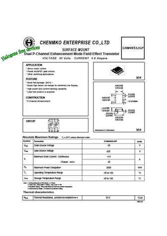
CHENMKO ENTERPRISE CO.,LTD CHM4953JGP SURFACE MOUNT Dual P-Channel Enhancement Mode Field Effect Transistor VOLTAGE 30 Volts CURRENT 4.9 Ampere APPLICATION * Servo motor control. * Power MOSFET gate drivers. * Other switching applications. SO-8 FEATURE * Small flat package. (SO-8 ) ( ) * Super high dense cell design for extremely low RDS(ON). 4.06 0.160 ( ) 3.70 0.146 * High ... See More ⇒
hm4953c.pdf
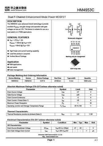
HM4953C Dual P-Channel Enhancement Mode Power MOSFET DESCRIPTION The HM4953C uses advanced trench technology to provide D D excellent RDS(ON), low gate charge and operation with gate voltages as low as 2.5V. This device is suitable for use as a G G load switch or in PWM applications. S S GENERAL FEATURES Schematic diagram VDS = -27V,ID = -5A RDS(ON) ... See More ⇒
hm4953.pdf

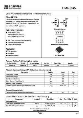
HM4953 Dual P-Channel Enhancement Mode Power MOSFET DESCRIPTION D1 D2 The HM4953 uses advanced trench technology to provide excellent RDS(ON), low gate charge and operation with gate G1 G2 voltages as low as 4.5V. This device is suitable for use as a load switch or in PWM applications. S1 S2 Schematic diagram GENERAL FEATURES VDS = -30V,ID = -5.1A RDS(ON) ... See More ⇒
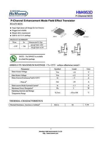
Detailed specifications: HM4886A, HM4886E, HM4887, HM4892A, HM4892B, HM4922, HM4953, HM4953A, IRF540, HM4953C, HM4953D, HM4963, HM4N10PR, HM4N150T, HM4N60, HM4N60F, HM4N60I
Keywords - HM4953B MOSFET specs
HM4953B cross reference
HM4953B equivalent finder
HM4953B pdf lookup
HM4953B substitution
HM4953B replacement
Can't find your MOSFET? Learn how to find a substitute transistor by analyzing voltage, current and package compatibility
🌐 : EN ES РУ

LIST
Last Update
MOSFET: AUN084N10 | AUN065N10 | AUN063N10 | AUN062N08BG | AUN060N08AG | AUN053N10 | AUN050N08BGL | AUN045N085 | AUN042N055 | AUN036N10
Popular searches
2n1304 | 2sa979 | 2sc4793 | d965 | mje15031 | irfp150n | mj15025 | mp1620