FDD6670S Datasheet. Specs and Replacement
Type Designator: FDD6670S 📄📄
Type of Transistor: MOSFET
Type of Control Channel: N-Channel
Absolute Maximum Ratings
Pd ⓘ - Maximum Power Dissipation: 70 W
|Vds|ⓘ - Maximum Drain-Source Voltage: 30 V
|Vgs|ⓘ - Maximum Gate-Source Voltage: 20 V
|Id| ⓘ - Maximum Drain Current: 64 A
Tj ⓘ - Maximum Junction Temperature: 150 °C
Electrical Characteristics
tr ⓘ - Rise Time: 10 nS
Cossⓘ - Output Capacitance: 526 pF
RDSonⓘ - Maximum Drain-Source On-State Resistance: 0.009 Ohm
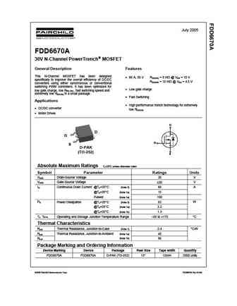
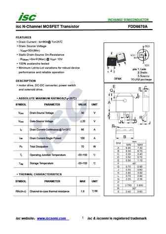
Package: TO252
FDD6670S substitution
- MOSFET ⓘ Cross-Reference Search
FDD6670S datasheet
fdd6670s.pdf
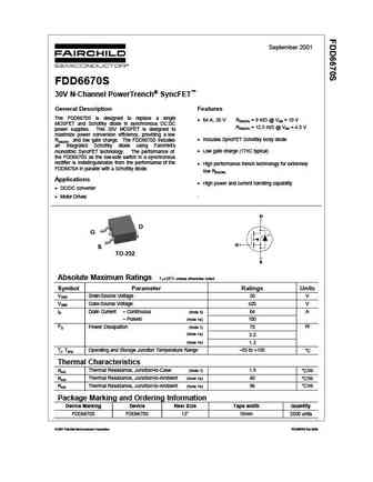
September 2001 FDD6670S 30V N-Channel PowerTrench SyncFET General Description Features The FDD6670S is designed to replace a single 64 A, 30 V RDS(ON) = 9 m @ VGS = 10 V MOSFET and Schottky diode in synchronous DC DC RDS(ON) = 12.5 m @ VGS = 4.5 V power supplies. This 30V MOSFET is designed to maximize power conversion efficiency, providing a low Includes S... See More ⇒
fdd6670s.pdf
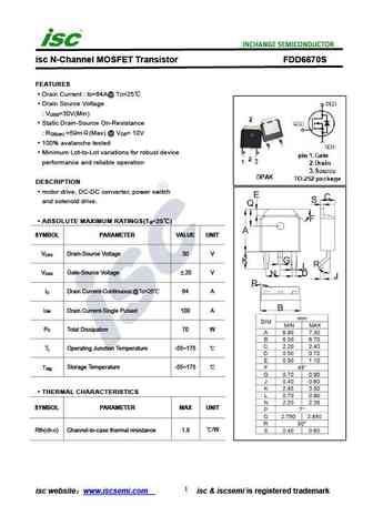
isc N-Channel MOSFET Transistor FDD6670S FEATURES Drain Current I =64A@ T =25 D C Drain Source Voltage V =30V(Min) DSS Static Drain-Source On-Resistance R =59m (Max) @ V = 10V DS(on) GS 100% avalanche tested Minimum Lot-to-Lot variations for robust device performance and reliable operation DESCRIPTION motor drive, DC-DC converter, power switch and solenoid d... See More ⇒
fdd6670al.pdf
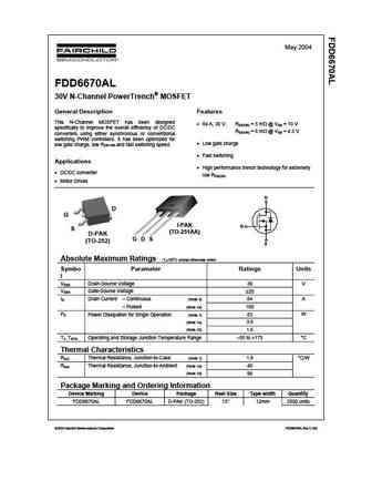
May 2004 FDD6670AL 30V N-Channel PowerTrench MOSFET General Description Features This N-Channel MOSFET has been designed 84 A, 30 V. RDS(ON) = 5 m @ VGS = 10 V specifically to improve the overall efficiency of DC/DC RDS(ON) = 6 m @ VGS = 4.5 V converters using either synchronous or conventional switching PWM controllers. It has been optimized for Low gate c... See More ⇒
fdd6670as.pdf
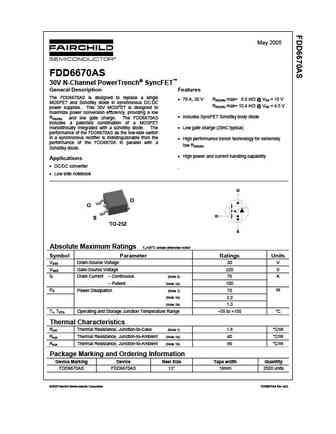
May 2005 FDD6670AS 30V N-Channel PowerTrench SyncFET General Description Features The FDD6670AS is designed to replace a single 76 A, 30 V RDS(ON) max= 8.0 m @ VGS = 10 V MOSFET and Schottky diode in synchronous DC DC RDS(ON) max= 10.4 m @ VGS = 4.5 V power supplies. This 30V MOSFET is designed to maximize power conversion efficiency, providing a low Inclu... See More ⇒

Detailed specifications: VS4620DS-G, VS4640DE, VSA007N02KD, SD2933W, FDD6030BL, FDD603AL, FDD6644, FDU6644, K2611, FDD6676, FDD6676S, FDD6680S, FDD6692, FDU6692, FDH20N40, FDP20N40, FDH34N40
Keywords - FDD6670S MOSFET specs
FDD6670S cross reference
FDD6670S equivalent finder
FDD6670S pdf lookup
FDD6670S substitution
FDD6670S replacement
Can't find your MOSFET? Learn how to find a substitute transistor by analyzing voltage, current and package compatibility
