ME15N25F Specs and Replacement
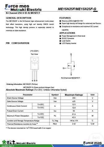
Type Designator: ME15N25F
Type of Transistor: MOSFET
Type of Control Channel: N-Channel
Absolute Maximum Ratings
Pd ⓘ - Maximum Power Dissipation: 61.9 W
|Vds|ⓘ - Maximum Drain-Source Voltage: 250 V
|Vgs|ⓘ - Maximum Gate-Source Voltage: 25 V
|Id| ⓘ - Maximum Drain Current: 12.5 A
Tj ⓘ - Maximum Junction Temperature: 175 °C
Electrical Characteristics
tr ⓘ - Rise Time: 43.4 nS
Cossⓘ - Output Capacitance: 118 pF
RDSonⓘ - Maximum Drain-Source On-State Resistance: 0.22 Ohm
Package: TO220F
ME15N25F substitution
- MOSFET ⓘ Cross-Reference Search
ME15N25F datasheet
me15n25f me15n25f-g.pdf
ME15N25F/ME15N25F-G N-Channel 250-V (D-S) MOSFET GENERAL DESCRIPTION FEATURES RDS(ON) 220m @VGS=10V The ME15N25F is the N-Channel logic enhancement mode power Super high density cell design for extremely low RDS(ON) field effect transistors, using high cell density, DMOS trench Exceptional on-resistance and maximum DC current technology. This high density process ... See More ⇒
me15n25 me15n25-g.pdf
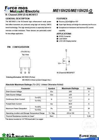
ME15N25/ME15N25-G N- Channel 250V (D-S) MOSFET GENERAL DESCRIPTION FEATURES The ME15N25 is the N-Channel logic enhancement mode power RDS(ON) 265m @VGS=10V field effect transistors are produced using high cell density, DMOS Super high density cell design for extremely low RDS(ON) trench technology. This high density process is especially tailored to Exceptional on-resi... See More ⇒
me15n10 me15n10g.pdf
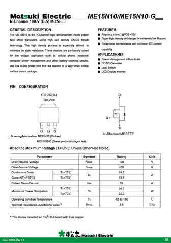
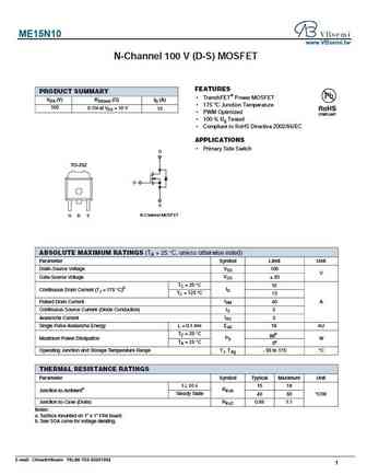
ME15N10/ME15N10-G N-Channel 100-V (D-S) MOSFET GENERAL DESCRIPTION FEATURES RDS(ON) 100m @VGS=10V The ME15N10 is the N-Channel logic enhancement mode power Super high density cell design for extremely low RDS(ON) field effect transistors, using high cell density, DMOS trench Exceptional on-resistance and maximum DC current technology. This high density process is ... See More ⇒
me15n10 me15n10-g.pdf
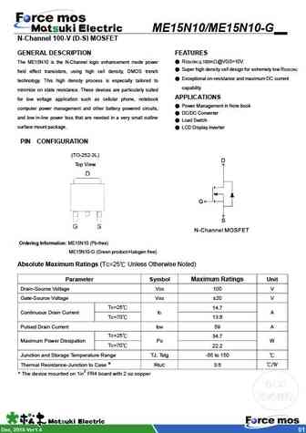
ME15N10/ME15N10-G N-Channel 100-V (D-S) MOSFET GENERAL DESCRIPTION FEATURES RDS(ON) 100m @VGS=10V The ME15N10 is the N-Channel logic enhancement mode power Super high density cell design for extremely low RDS(ON) field effect transistors, using high cell density, DMOS trench Exceptional on-resistance and maximum DC current technology. This high density process is ... See More ⇒
Detailed specifications: ME120N04T, ME1302AT3, ME1302AT3-G, ME1303AT3, ME1303AT3-G, ME13N10A, ME13N10A-G, ME15N25, 10N60, ME15N25F-G, ME15N25-G, ME200N04T, ME200N04T-G, ME20N10-G, ME20N15F, ME2301A, ME2301A-G
Keywords - ME15N25F MOSFET specs
ME15N25F cross reference
ME15N25F equivalent finder
ME15N25F pdf lookup
ME15N25F substitution
ME15N25F replacement
Step-by-step guide to finding a MOSFET replacement. Cross-reference parts and ensure compatibility for your repair or project.
