ME2301S Specs and Replacement
Type Designator: ME2301S
Type of Transistor: MOSFET
Type of Control Channel: P-Channel
Absolute Maximum Ratings
Pd ⓘ - Maximum Power Dissipation: 1.3 W
|Vds|ⓘ - Maximum Drain-Source Voltage: 20 V
|Vgs|ⓘ - Maximum Gate-Source Voltage: 8 V
|Id| ⓘ - Maximum Drain Current: 2.8 A
Tj ⓘ - Maximum Junction Temperature: 150 °C
Electrical Characteristics
tr ⓘ - Rise Time: 26 nS
Cossⓘ - Output Capacitance: 56 pF
RDSonⓘ - Maximum Drain-Source On-State Resistance: 0.11 Ohm
Package: SOT23
ME2301S substitution
- MOSFET ⓘ Cross-Reference Search
ME2301S datasheet
me2301s me2301s-g.pdf
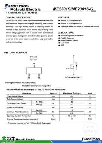
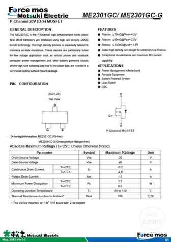
ME2301S/ME2301S-G P-Channel 20V (D-S) MOSFET GENERAL DESCRIPTION FEATURES RDS(ON) 110m @VGS=-4.5V The ME2301S is the P-Channel logic enhancement mode power field RDS(ON) 150m @VGS=-2.5V effect transistors are produced using high cell density , DMOS trench Super high density cell design for extremely low RDS(ON) technology. This high density process is espec... See More ⇒
me2301a me2301a-g.pdf
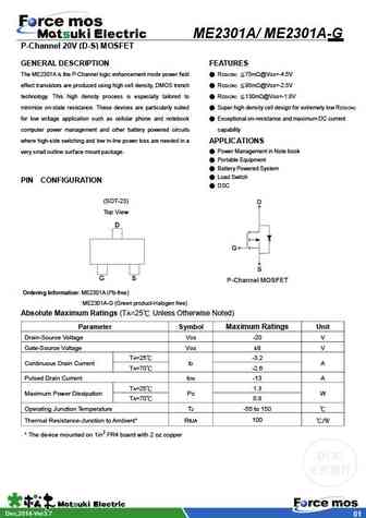
ME2301A/ ME2301A-G P-Channel 20V (D-S) MOSFET GENERAL DESCRIPTION FEATURES The ME2301A is the P-Channel logic enhancement mode power field RDS(ON) 75m @VGS=-4.5V effect transistors are produced using high cell density, DMOS trench RDS(ON) 95m @VGS=-2.5V technology. This high density process is especially tailored to RDS(ON) 130m @VGS=-1.8V minimize on-stat... See More ⇒
me2301 me2301-g.pdf
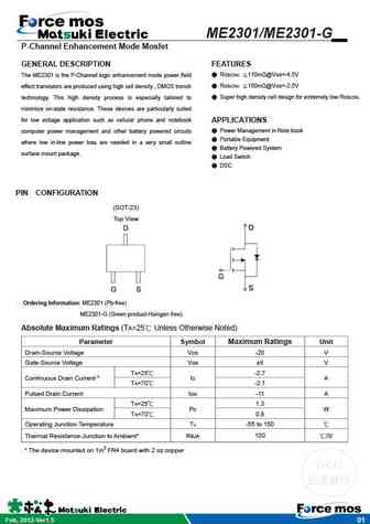
ME2301/ME2301-G P-Channel Enhancement Mode Mosfet GENERAL DESCRIPTION FEATURES RDS(ON) 110m @VGS=-4.5V The ME2301 is the P-Channel logic enhancement mode power field RDS(ON) 150m @VGS=-2.5V effect transistors are produced using high cell density , DMOS trench Super high density cell design for extremely low RDS(ON) technology. This high density process is es... See More ⇒
me2301dc me2301dc-g.pdf
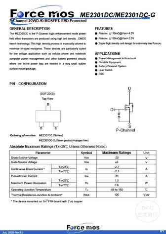
ME2301DC/ME2301DC-G P-Channel 20V(D-S) MOSFET, ESD Protected GENERAL DESCRIPTION FEATURES The ME2301DC is the P-Channel logic enhancement mode power RDS(ON) 110m @VGS=-4.5V field effect transistors are produced using high cell density , DMOS RDS(ON) 150m @VGS=-2.5V trench technology. This high density process is especially tailored to Super high density cell design ... See More ⇒
Detailed specifications: ME2301A, ME2301A-G, ME2301DC, ME2301DC-G, ME2301DN, ME2301DN-G, ME2301GC, ME2301GC-G, IRF4905, ME2301S-G, ME2302-G, ME2303, ME2303-G, ME2305, ME2305A, ME2305A-G, ME2305-G
Keywords - ME2301S MOSFET specs
ME2301S cross reference
ME2301S equivalent finder
ME2301S pdf lookup
ME2301S substitution
ME2301S replacement
Can't find your MOSFET? Learn how to find a substitute transistor by analyzing voltage, current and package compatibility
