ME2305A-G Specs and Replacement
Type Designator: ME2305A-G
Type of Transistor: MOSFET
Type of Control Channel: P-Channel
Absolute Maximum Ratings
Pd ⓘ
- Maximum Power Dissipation: 1.3 W
|Vds|ⓘ - Maximum Drain-Source Voltage: 20 V
|Vgs|ⓘ - Maximum Gate-Source Voltage: 8 V
|Id| ⓘ - Maximum Drain Current: 3.5 A
Tj ⓘ - Maximum Junction Temperature: 150 °C
Electrical Characteristics
tr ⓘ - Rise Time: 18 nS
Cossⓘ -
Output Capacitance: 65 pF
RDSonⓘ - Maximum Drain-Source On-State Resistance: 0.067 Ohm
Package: SOT23
- MOSFET ⓘ Cross-Reference Search
ME2305A-G datasheet
..1. Size:1057K matsuki electric
me2305a me2305a-g.pdf 
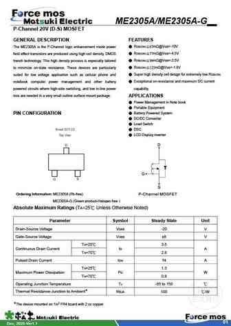
ME2305A/ME2305A-G P-Channel 20V (D-S) MOSFET GENERAL DESCRIPTION FEATURES The ME2305A is the P-Channel logic enhancement mode power RDS(ON) 67m @VGS=-10V field effect transistors are produced using high cell density, DMOS RDS(ON) 77m @VGS=-4.5V trench technology. This high density process is especially tailored RDS(ON) 96m @VGS=-2.5V to minimize on-state resistan... See More ⇒
8.1. Size:1136K matsuki electric
me2305 me2305-g.pdf
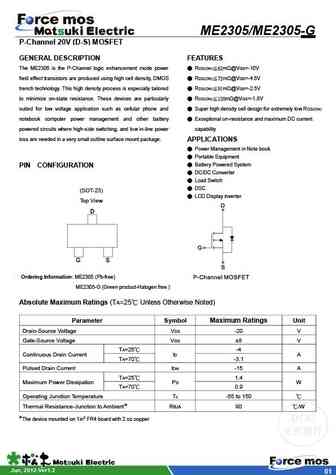
ME2305/ME2305-G P-Channel 20V (D-S) MOSFET GENERAL DESCRIPTION FEATURES The ME2305 is the P-Channel logic enhancement mode power RDS(ON) 62m @VGS=-10V field effect transistors are produced using high cell density, DMOS RDS(ON) 72m @VGS=-4.5V trench technology. This high density process is especially tailored RDS(ON) 91m @VGS=-2.5V to minimize on-state resista... See More ⇒
9.1. Size:1599K matsuki electric
me2306bs me2306bs-g.pdf
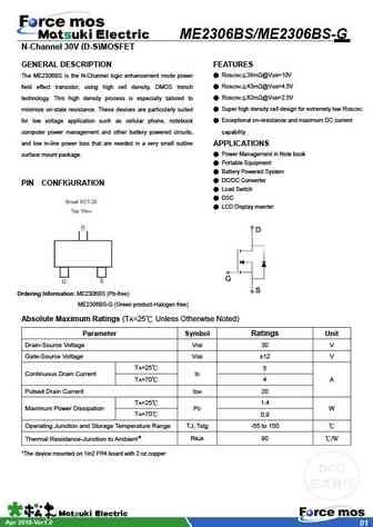
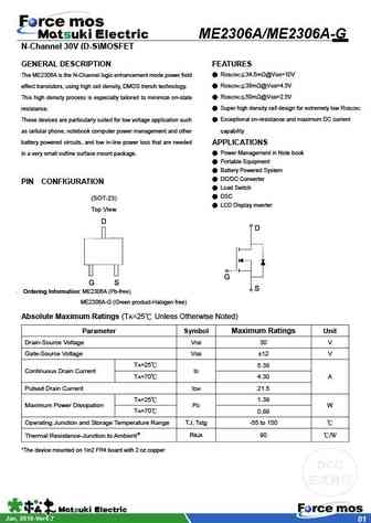
ME2306BS/ME2306BS-G N-Channel 30V (D-S)MOSFET GENERAL DESCRIPTION FEATURES The ME2306BS is the N-Channel logic enhancement mode power RDS(ON) 38m @VGS=10V field effect transistor, using high cell density, DMOS trench RDS(ON) 43m @VGS=4.5V technology. This high density process is especially tailored to RDS(ON) 62m @VGS=2.5V minimize on-state resistance. These ... See More ⇒
9.2. Size:879K matsuki electric
me2306n me2306n-g.pdf
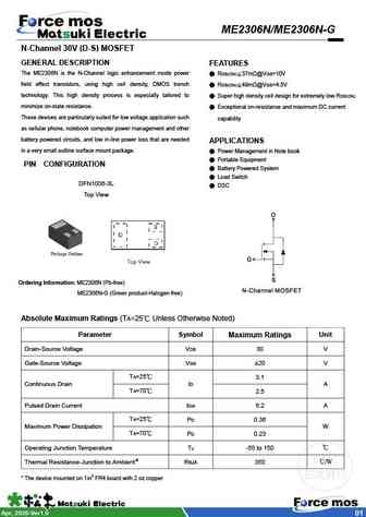
ME2306N/ME2306N-G N-Channel 30V (D-S) MOSFET GENERAL DESCRIPTION FEATURES The ME2306N is the N-Channel logic enhancement mode power RDS(ON) 37m @VGS=10V field effect transistors, using high cell density, DMOS trench RDS(ON) 49m @VGS=4.5V technology. This high density process is especially tailored to Super high density cell design for extremely low RDS(ON) mi... See More ⇒
9.3. Size:1077K matsuki electric
me2301a me2301a-g.pdf
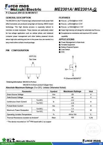
ME2301A/ ME2301A-G P-Channel 20V (D-S) MOSFET GENERAL DESCRIPTION FEATURES The ME2301A is the P-Channel logic enhancement mode power field RDS(ON) 75m @VGS=-4.5V effect transistors are produced using high cell density, DMOS trench RDS(ON) 95m @VGS=-2.5V technology. This high density process is especially tailored to RDS(ON) 130m @VGS=-1.8V minimize on-stat... See More ⇒
9.4. Size:1127K matsuki electric
me2301 me2301-g.pdf
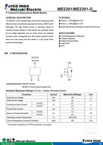
ME2301/ME2301-G P-Channel Enhancement Mode Mosfet GENERAL DESCRIPTION FEATURES RDS(ON) 110m @VGS=-4.5V The ME2301 is the P-Channel logic enhancement mode power field RDS(ON) 150m @VGS=-2.5V effect transistors are produced using high cell density , DMOS trench Super high density cell design for extremely low RDS(ON) technology. This high density process is es... See More ⇒
9.5. Size:976K matsuki electric
me2303 me2303-g.pdf
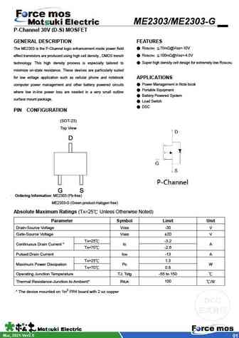
ME2303/ME2303-G P-Channel 30V (D-S) MOSFET GENERAL DESCRIPTION FEATURES The ME2303 is the P-Channel logic enhancement mode power field RDS(ON) 75m @VGS=-10V effect transistors are produced using high cell density , DMOS trench RDS(ON) 100m @VGS=-4.5V technology. This high density process is especially tailored to Super high density cell design for extremely low RDS(... See More ⇒
9.6. Size:1294K matsuki electric
me2306s me2306s-g.pdf
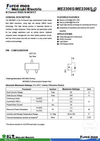
ME2306S/ME2306S-G N-Channel 30V(D-S) MOSFET GENERAL DESCRIPTION FEATURES FEATURES RDS(ON) 37m @ VGS =10V The ME2306S is the N-Channel logic enhancement mode power RDS(ON) 49m @VGS=4.5V field effect transistors, using high cell density, DMOS trench Super high density cell design for extremely low RDS(ON) technology. This high density process is especially tailor... See More ⇒
9.7. Size:587K matsuki electric
me2302.pdf
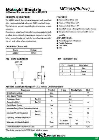
ME2302(Pb-free) N-Channel Enhancement Mode MOSFET GENERAL DESCRIPTION FEATURES The ME2302 is the N-Channel logic enhancement mode power field RDS(ON) 85m @VGS=4.5V effect transistors, using high cell density, DMOS trench technology. RDS(ON) 115m @VGS=2.5V This high density process is especially tailored to minimize on-state RDS(ON) 135m @VGS=1.8V resistance. ... See More ⇒
9.8. Size:730K matsuki electric
me2306an me2306an-g.pdf
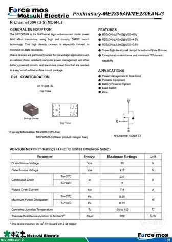
Preliminary-ME2306AN/ME2306AN-G N-Channel 30V (D-S) MOSFET GENERAL DESCRIPTION FEATURES The ME2306AN is the N-Channel logic enhancement mode power RDS(ON) 37m @VGS=10V field effect transistors, using high cell density, DMOS trench RDS(ON) 40m @VGS=4.5V technology. This high density process is especially tailored to RDS(ON) 53m @VGS=2.5V minimize on-state r... See More ⇒
9.9. Size:1115K matsuki electric
me2306ds me2306ds-g.pdf
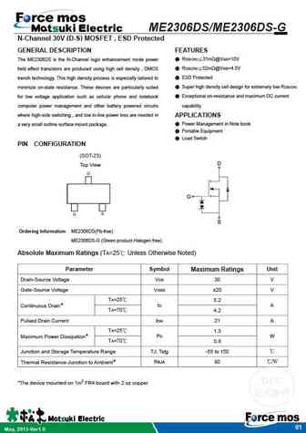
ME2306DS/ME2306DS-G N-Channel 30V (D-S) MOSFET , ESD Protected GENERAL DESCRIPTION FEATURES The ME2306DS is the N-Channel logic enhancement mode power RDS(ON) 31m @VGS=10V field effect transistors are produced using high cell density , DMOS RDS(ON) 52m @VGS=4.5V trench technology. This high density process is especially tailored to ESD Protected minimize on-state ... See More ⇒
9.10. Size:1999K matsuki electric
me2301dc me2301dc-g.pdf
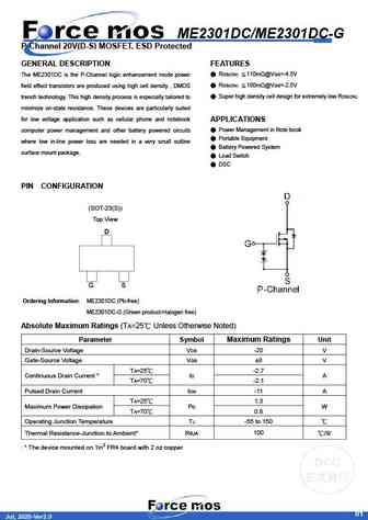
ME2301DC/ME2301DC-G P-Channel 20V(D-S) MOSFET, ESD Protected GENERAL DESCRIPTION FEATURES The ME2301DC is the P-Channel logic enhancement mode power RDS(ON) 110m @VGS=-4.5V field effect transistors are produced using high cell density , DMOS RDS(ON) 150m @VGS=-2.5V trench technology. This high density process is especially tailored to Super high density cell design ... See More ⇒
9.11. Size:1540K matsuki electric
me2308s me2308s-g.pdf
ME2308S/ME2308S-G N-Channel 60V (D-S) MOSFET GENERAL DESCRIPTION FEATURES The ME2308S is the N-Channel logic enhancement mode power RDS(ON) 100m @VGS=10V field effect transistors are produced using high cell density, DMOS RDS(ON) 130m @VGS=4.5V trench technology. This high density process is especially tailored to Super high density cell design for extremely low RDS... See More ⇒
9.12. Size:1321K matsuki electric
me2301gc me2301gc-g.pdf
ME2301GC/ ME2301GC-G P-Channel 20V (D-S) MOSFET GENERAL DESCRIPTION FEATURES RDS(ON) 75m @VGS=-4.5V The ME2301GC is the P-Channel logic enhancement mode power RDS(ON) 95m @VGS=-2.5V field effect transistors are produced using high cell density, DMOS RDS(ON) 130m @VGS=-1.8V trench technology. This high density process is especially tailored to Sup... See More ⇒
9.13. Size:1298K matsuki electric
me2301dn me2301dn-g.pdf
ME2301DN/ME2301DN-G P-Channel 20V(D-S) MOSFET, ESD Protected GENERAL DESCRIPTION FEATURES The ME2301DN is the P-Channel logic enhancement mode power RDS(ON) 90m @VGS=-4.5V field effect transistors are produced using high cell density , DMOS RDS(ON) 130m @VGS=-2.5V trench technology. This high density process is especially tailored to Super high density cell desig... See More ⇒
9.14. Size:1039K matsuki electric
me2306as me2306as-g.pdf
ME2306AS/ME2306AS-G N-Channel 30V (D-S)MOSFET GENERAL DESCRIPTION FEATURES The ME2306AS is the N-Channel logic enhancement mode power RDS(ON) 34.5m @VGS=10V field effect transistors, using high cell density, DMOS trench RDS(ON) 38m @VGS=4.5V technology.This high density process is especially tailored to RDS(ON) 50m @VGS=2.5V minimize on-state resistance.These... See More ⇒
9.15. Size:1718K matsuki electric
me2307 me2307-g.pdf
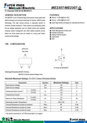
ME2307/ME2307-G P-Channel 30V (D-S) MOSFET GENERAL DESCRIPTION FEATURES The ME2307 is the P-Channel logic enhancement mode power field RDS(ON) 70m @VGS=-10V effect transistors are produced using high cell density , DMOS trench RDS(ON) 95m @VGS=-4.5V technology. This high density process is especially tailored to Super high density cell design for extremely low RDS(O... See More ⇒
9.16. Size:1070K matsuki electric
me2309 me2309-g.pdf
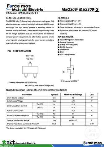
ME2309/ ME2309-G P-Channel 60V (D-S) MOSFET GENERAL DESCRIPTION FEATURES The ME2309 is the P-Channel logic enhancement mode power field RDS(ON) 215m @VGS=-10V effect transistors are produced using high cell density, DMOS trench RDS(ON) 260m @VGS=-4.5V technology. This high density process is especially tailored to Super high density cell design for extremely low RDS(O... See More ⇒
9.17. Size:1457K matsuki electric
me2306d me2306d-g.pdf
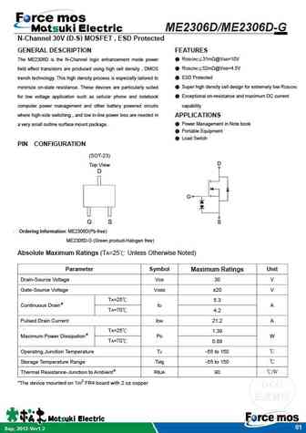
ME2306D/ME2306D-G N-Channel 30V (D-S) MOSFET , ESD Protected GENERAL DESCRIPTION FEATURES The ME2306D is the N-Channel logic enhancement mode power RDS(ON) 31m @VGS=10V field effect transistors are produced using high cell density , DMOS RDS(ON) 52m @VGS=4.5V trench technology. This high density process is especially tailored to ESD Protected minimize on-state res... See More ⇒
9.18. Size:1432K matsuki electric
me2302 me2302-g.pdf
ME2302/ME2302-G N-Channel 20V(D-S) MOSFET GENERAL DESCRIPTION FEATURES The ME2302 is the N-Channel logic enhancement mode power field RDS(ON) 85m @VGS=4.5V effect transistors, using high cell density, DMOS trench technology. RDS(ON) 115m @VGS=2.5V This high density process is especially tailored to minimize on-state RDS(ON) 130m @VGS=1.8V resistance.T... See More ⇒
9.19. Size:1009K matsuki electric
me2301s me2301s-g.pdf
ME2301S/ME2301S-G P-Channel 20V (D-S) MOSFET GENERAL DESCRIPTION FEATURES RDS(ON) 110m @VGS=-4.5V The ME2301S is the P-Channel logic enhancement mode power field RDS(ON) 150m @VGS=-2.5V effect transistors are produced using high cell density , DMOS trench Super high density cell design for extremely low RDS(ON) technology. This high density process is espec... See More ⇒
9.20. Size:1045K matsuki electric
me2306 me2306-g.pdf
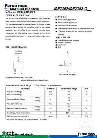
ME2306/ME2306-G N-Channel Enhancement Mode MOSFET GENERAL DESCRIPTION FEATURES RDS(ON) 37m @VGS=10V The ME2306 is the N-Channel logic enhancement mode power field RDS(ON) 49m @VGS=4.5V effect transistors, using high cell density, DMOS trench technology. Super high density cell design for extremely low RDS(ON) This high density process is especially tailored to... See More ⇒
9.21. Size:921K matsuki electric
me2308d me2308d-g.pdf
ME2308D/ME2308D-G N-Channel 30V (D-S) MOSFET ,ESD Protection GENERAL DESCRIPTION FEATURES The ME2308D is the N-Channel logic enhancement mode power RDS(ON) 60m @VGS=10V field effect transistors are produced using high cell density, DMOS RDS(ON) 70m @VGS=4.5V trench technology. This high density process is especially tailored to RDS(ON) 100m @VGS=2.5V minimize... See More ⇒
9.22. Size:830K matsuki electric
me2308dn-g.pdf
ME2308DN-G N-Channel 20V (D-S) MOSFET ,ESD Protection GENERAL DESCRIPTION FEATURES The ME2308DN-G is the N-Channel logic enhancement mode power RDS(ON) 0.35 @VGS=4.5V field effect transistors are produced using high cell density, DMOS RDS(ON) 0.45 @VGS=2.5V trench technology. This high density process is especially tailored to RDS(ON) 0.65 @VGS=1.8V mini... See More ⇒
9.23. Size:1203K matsuki electric
me2306a me2306a-g.pdf
ME2306A/ME2306A-G N-Channel 30V (D-S)MOSFET GENERAL DESCRIPTION FEATURES The ME2306A is the N-Channel logic enhancement mode power field RDS(ON) 34.5m @VGS=10V effect transistors, using high cell density, DMOS trench technology. RDS(ON) 38m @VGS=4.5V This high density process is especially tailored to minimize on-state RDS(ON) 50m @VGS=2.5V resistance. Su... See More ⇒
9.24. Size:850K cn vbsemi
me2308s.pdf
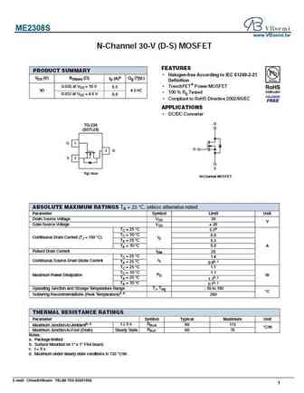
ME2308S www.VBsemi.tw N-Channel 30-V (D-S) MOSFET FEATURES PRODUCT SUMMARY Halogen-free According to IEC 61249-2-21 VDS (V) RDS(on) ( ) ID (A)a Qg (Typ.) Definition 0.030 at VGS = 10 V TrenchFET Power MOSFET 6.5 30 4.5 nC 100 % Rg Tested 0.033 at VGS = 4.5 V 6.0 Compliant to RoHS Directive 2002/95/EC APPLICATIONS DC/DC Converter D TO-236 (SOT-23) G ... See More ⇒
Detailed specifications: ME2301GC-G, ME2301S, ME2301S-G, ME2302-G, ME2303, ME2303-G, ME2305, ME2305A, SKD502T, ME2305-G, ME2306, ME2306AN, ME2306AN-G, ME2306AS, ME2306AS-G, ME2306BS, ME2306BS-G
Keywords - ME2305A-G MOSFET specs
ME2305A-G cross reference
ME2305A-G equivalent finder
ME2305A-G pdf lookup
ME2305A-G substitution
ME2305A-G replacement
Need a MOSFET replacement?
Our guide shows you how to find a perfect substitute by comparing key parameters and specs
