MEE3712F Specs and Replacement
Type Designator: MEE3712F
Type of Transistor: MOSFET
Type of Control Channel: N-Channel
Absolute Maximum Ratings
Pd ⓘ - Maximum Power Dissipation: 36.7 W
|Vds|ⓘ - Maximum Drain-Source Voltage: 100 V
|Vgs|ⓘ - Maximum Gate-Source Voltage: 20 V
|Id| ⓘ - Maximum Drain Current: 31 A
Tj ⓘ - Maximum Junction Temperature: 150 °C
Electrical Characteristics
tr ⓘ - Rise Time: 21 nS
Cossⓘ - Output Capacitance: 572 pF
RDSonⓘ - Maximum Drain-Source On-State Resistance: 0.018 Ohm
Package: TO220F
MEE3712F substitution
- MOSFET ⓘ Cross-Reference Search
MEE3712F datasheet
mee3712f.pdf
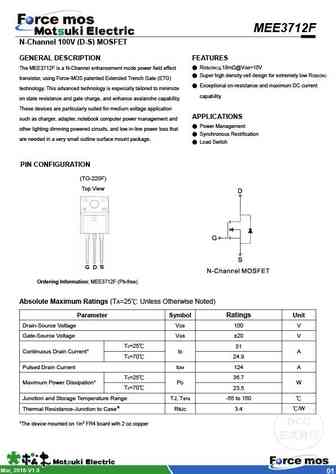
MEE3712F N-Channel 100V (D-S) MOSFET GENERAL DESCRIPTION FEATURES RDS(ON) 18m @VGS=10V The MEE3712F is a N-Channel enhancement mode power field effect Super high density cell design for extremely low RDS(ON) transistor, using Force-MOS patented Extended Trench Gate (ETG) Exceptional on-resistance and maximum DC current technology. This advanced technology is espec... See More ⇒
mee3712t.pdf

MEE3712T N-Channel 100V (D-S) MOSFET GENERAL DESCRIPTION FEATURES RDS(ON) 18m @VGS=10V The MEE3712T is a N-Channel enhancement mode power field effect Super high density cell design for extremely low RDS(ON) transistor, using Force-MOS patented Extended Trench Gate (ETG) Exceptional on-resistance and maximum DC current technology. This advanced technology is espec... See More ⇒
mee3712h.pdf
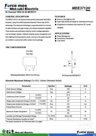
MEE3712H N-Channel 100V (D-S) MOSFET GENERAL DESCRIPTION FEATURES RDS(ON) 18m @VGS=10V The MEE3712H is a N-Channel enhancement mode power field effect Super high density cell design for extremely low RDS(ON) transistor, using Force-MOS patented Extended Trench Gate (ETG) Exceptional on-resistance and maximum DC current technology. This advanced technology is espec... See More ⇒
mee3710t.pdf
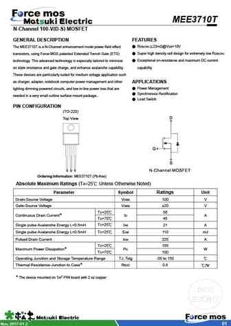
MEE3710T N-Channel 100-V(D-S) MOSFET GENERAL DESCRIPTION FEATURES The MEE3710T is a N-Channel enhancement mode power field effect RDS(ON) 23m @VGS=10V transistors, using Force-MOS patented Extended Trench Gate (ETG) Super high density cell design for extremely low RDS(ON) technology. This advanced technology is especially tailored to minimize Exceptional on-resistance ... See More ⇒
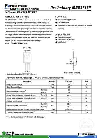
Detailed specifications: ME9435AS, ME9435AS-G, ME95N10F, ME95N10F-G, ME96N03-G, MEE2348, MEE2348-G, MEE3710T, AO3400, MEE3712H, MEE3712T, MEE3716F, MEE3716T, MEE3718T, MEE4292-G, MEE4292HP-G, MEE4292HT
Keywords - MEE3712F MOSFET specs
MEE3712F cross reference
MEE3712F equivalent finder
MEE3712F pdf lookup
MEE3712F substitution
MEE3712F replacement
Learn how to find the right MOSFET substitute. A guide to cross-reference, check specs and replace MOSFETs in your circuits.
🌐 : EN ES РУ

LIST
Last Update
MOSFET: AUB062N08BG | AUB060N08AG | AUB056N10 | AUB056N08BGL | AUB050N085 | AUB050N055 | AUB045N12 | AUB045N10BT | AUB039N10 | AUB034N10
Popular searches
2sa720 | 2sc1345 | 2sd555 | a950 transistor | k2611 | c1740 transistor | c828 transistor | c4467