TMD6N70G Datasheet. Specs and Replacement
Type Designator: TMD6N70G
Type of Transistor: MOSFET
Type of Control Channel: N-Channel
Absolute Maximum Ratings
Pd ⓘ - Maximum Power Dissipation: 120 W
|Vds|ⓘ - Maximum Drain-Source Voltage: 700 V
|Vgs|ⓘ - Maximum Gate-Source Voltage: 30 V
|Id| ⓘ - Maximum Drain Current: 5 A
Tj ⓘ - Maximum Junction Temperature: 150 °C
Electrical Characteristics
tr ⓘ - Rise Time: 17 nS
Cossⓘ - Output Capacitance: 91 pF
RDSonⓘ - Maximum Drain-Source On-State Resistance: 1.65 Ohm
Package: DPAK
TMD6N70G substitution
- MOSFET ⓘ Cross-Reference Search
TMD6N70G datasheet
tmd6n70g tmu6n70g tmd6n70 tmu6n70.pdf

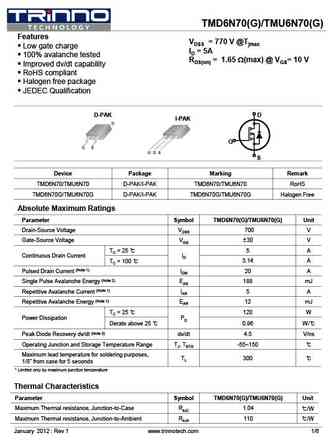
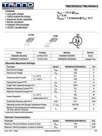
TMD6N70(G)/TMU6N70(G) Features VDSS = 770 V @Tjmax Low gate charge ID = 5A 100% avalanche tested RDS(on) = 1.65 W(max) @ VGS= 10 V Improved dv/dt capability RoHS compliant Halogen free package JEDEC Qualification D-PAK D I-PAK G S Device Package Marking Remark TMD6N70/TMU6N70 D-PAK/I-PAK TMD6N70/TMU6N70 RoHS TMD6N70G/TMU6N70G D-PAK/I-PAK... See More ⇒
tmd6n70.pdf
TMD6N70(G)/TMU6N70(G) Features VDSS = 770 V @Tjmax Low gate charge ID = 5A 100% avalanche tested RDS(on) = 1.65 W(max) @ VGS= 10 V Improved dv/dt capability RoHS compliant Halogen free package JEDEC Qualification D-PAK D I-PAK G S Device Package Marking Remark TMD6N70/TMU6N70 D-PAK/I-PAK TMD6N70/TMU6N70 RoHS TMD6N70G/TMU6N70G D-PAK/I-PAK... See More ⇒
ntmd6n03r2.pdf
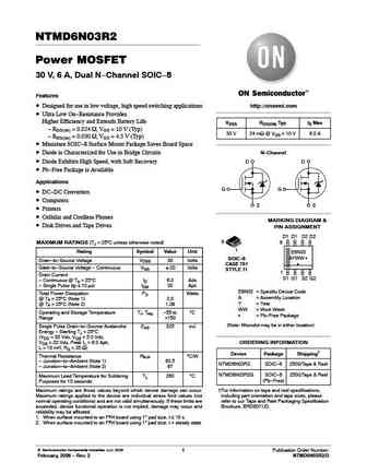
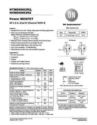
NTMD6N03R2 Power MOSFET 30 V, 6 A, Dual N-Channel SOIC-8 Features Designed for use in low voltage, high speed switching applications http //onsemi.com Ultra Low On-Resistance Provides Higher Efficiency and Extends Battery Life VDSS RDS(ON) Typ ID Max - RDS(on) = 0.024 W, VGS = 10 V (Typ) 30 V 24 mW @ VGS = 10 V 6.0 A - RDS(on) = 0.030 W, VGS = 4.5 V (Typ) Miniature SOIC-8... See More ⇒
ntmd6n02r2-d.pdf
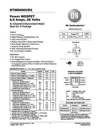
NTMD6N02R2 Power MOSFET 6.0 Amps, 20 Volts N-Channel Enhancement Mode Dual SO-8 Package http //onsemi.com Features VDSS RDS(ON) TYP ID MAX Ultra Low RDS(on) 20 V 35 mW @ VGS = 4.5 V 6.0 A Higher Efficiency Extending Battery Life Logic Level Gate Drive Miniature Dual SOIC-8 Surface Mount Package N-Channel Diode Exhibits High Speed, Soft Recovery D Avalanch... See More ⇒
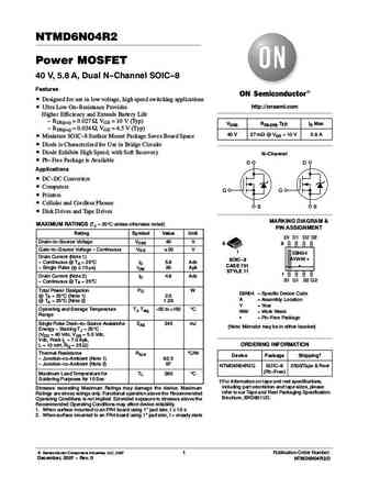
Detailed specifications: HRU120N10K, HRU180N10K, HRU50N06K, HRU72N06K, HRU80N06K, HRW370N10K, HN75N09AP, TMU6N70, IRFB4227, TMU6N70G, OSG07N65AF, OSG07N65DF, OSG07N65FF, OSG07N65PF, OSG50R1K5AF, OSG50R1K5DF, OSG50R1K5FF
Keywords - TMD6N70G MOSFET specs
TMD6N70G cross reference
TMD6N70G equivalent finder
TMD6N70G pdf lookup
TMD6N70G substitution
TMD6N70G replacement
Need a MOSFET replacement? Our guide shows you how to find a perfect substitute by comparing key parameters and specs
🌐 : EN ES РУ

LIST
Last Update
MOSFET: ASDM7002EZA | ASDM68N80KQ | ASDM6802ZC | ASDM60R042NQ | ASDM60P12KQ | ASDM60N80KQ | ASDM60N70Q | ASDM60N50KQ | ASDM60N45KQ | ASDM60N30KQ
Popular searches
2n2924 | mpsa65 | 2sa794 | 2sa816 | 2sc897 datasheet | 2sd389 | mp41 transistor | nkt275 datasheet