FDZ192NZ Specs and Replacement
Type Designator: FDZ192NZ
Type of Transistor: MOSFET
Type of Control Channel: N-Channel
Absolute Maximum Ratings
Pd ⓘ - Maximum Power Dissipation: 1.9 W
|Vds|ⓘ - Maximum Drain-Source Voltage: 20 V
|Vgs|ⓘ - Maximum Gate-Source Voltage: 8 V
|Id| ⓘ - Maximum Drain Current: 5.3 A
Tj ⓘ - Maximum Junction Temperature: 150 °C
Electrical Characteristics
RDSonⓘ - Maximum Drain-Source On-State Resistance: 0.039 Ohm
Package: WLCSP
FDZ192NZ substitution
- MOSFET ⓘ Cross-Reference Search
FDZ192NZ datasheet
fdz192nz.pdf
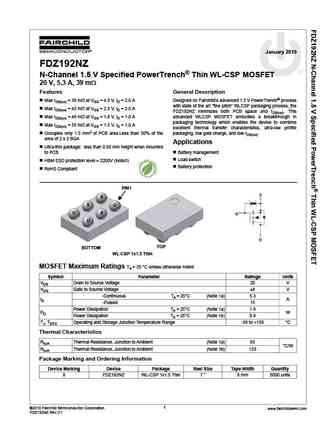
January 2010 FDZ192NZ N-Channel 1.5 V Specified PowerTrench Thin WL-CSP MOSFET 20 V, 5.3 A, 39 m Features General Description Max rDS(on) = 39 m at VGS = 4.5 V, ID = 2.0 A Designed on Fairchild's advanced 1.5 V PowerTrench process with state of the art "fine pitch" WLCSP packaging process, the Max rDS(on) = 43 m at VGS = 2.5 V, ID = 2.0 A FDZ192NZ minimizes both PCB sp... See More ⇒
fdz191p.pdf

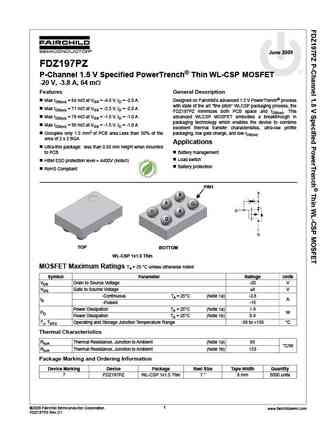
June 2009 FDZ191P P-Channel 1.5V PowerTrench WL-CSP MOSFET -20V, -1A, 85m Features General Description Designed on Fairchild's advanced 1.5V PowerTrench process Max rDS(on) = 85m at VGS = -4.5V, ID = -1A with state of the art "low pitch" WLCSP packaging process, the Max rDS(on) = 123m at VGS = -2.5V, ID = -1A FDZ191P minimizes both PCB space and rDS(on). This advanced WL... See More ⇒
fdz1905pz.pdf
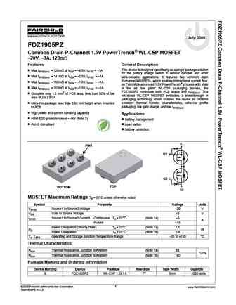
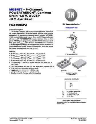
July 2008 FDZ1905PZ tm Common Drain P-Channel 1.5V PowerTrench WL-CSP MOSFET 20V, 3A, 123m Features General Description This device is designed specifically as a single package solution Max rS1S2(on) = 126m at VGS = 4.5V, IS1S2 = 1A for the battery charge switch in cellular handset and other Max rS1S2(on) = 141m at VGS = 2.5V, IS1S2 = 1A ultra-portab... See More ⇒
fdz193p.pdf
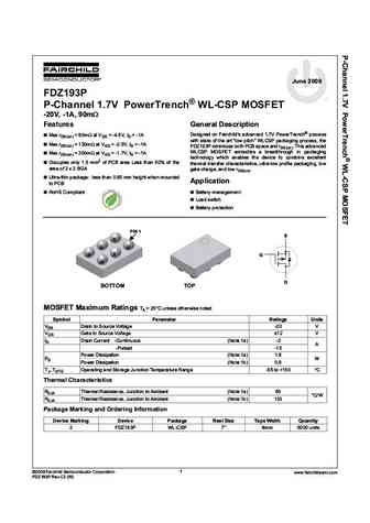
June 2009 FDZ193P tm P-Channel 1.7V PowerTrench WL-CSP MOSFET -20V, -1A, 90m Features General Description Designed on Fairchild's advanced 1.7V PowerTrench process Max rDS(on) = 90m at VGS = -4.5V, ID = -1A with state of the art "low pitch" WLCSP packaging process, the Max rDS(on) = 130m at VGS = -2.5V, ID = -1A FDZ193P minimizes both PCB space and rDS(on). This adva... See More ⇒
Detailed specifications: FDY3000NZ, FDY300NZ, FDY301NZ, FDY302NZ, FDY4000CZ, SDT02N02, FDZ1905PZ, FDZ191P, IRLB4132, FDZ193P, FDZ197PZ, FDZ371PZ, FDZ372NZ, FDZ375P, FDZ391P, FQA10N80CF109, SDF08N50
Keywords - FDZ192NZ MOSFET specs
FDZ192NZ cross reference
FDZ192NZ equivalent finder
FDZ192NZ pdf lookup
FDZ192NZ substitution
FDZ192NZ replacement
Step-by-step guide to finding a MOSFET replacement. Cross-reference parts and ensure compatibility for your repair or project.
🌐 : EN ES РУ

LIST
Last Update
MOSFET: AUN084N10 | AUN065N10 | AUN063N10 | AUN062N08BG | AUN060N08AG | AUN053N10 | AUN050N08BGL | AUN045N085 | AUN042N055 | AUN036N10
Popular searches
2024ont | 2n1306 transistor | 2sa750 datasheet | 2sa940 transistor datasheet | 2sb549 | 5n50 mosfet equivalent | a1016 transistor | a1693 transistor