NCE01P30I Specs and Replacement
Type Designator: NCE01P30I
Type of Transistor: MOSFET
Type of Control Channel: P-Channel
Absolute Maximum Ratings
Pd ⓘ - Maximum Power Dissipation: 120 W
|Vds|ⓘ - Maximum Drain-Source Voltage: 100 V
|Vgs|ⓘ - Maximum Gate-Source Voltage: 20 V
|Id| ⓘ - Maximum Drain Current: 30 A
Tj ⓘ - Maximum Junction Temperature: 175 °C
Electrical Characteristics
tr ⓘ - Rise Time: 80 nS
Cossⓘ - Output Capacitance: 184.5 pF
RDSonⓘ - Maximum Drain-Source On-State Resistance: 0.065 Ohm
Package: TO-251
NCE01P30I substitution
- MOSFET ⓘ Cross-Reference Search
NCE01P30I datasheet
nce01p30i.pdf
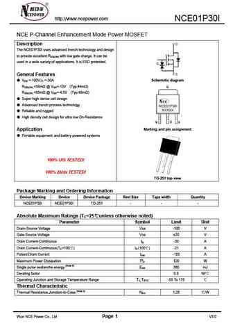
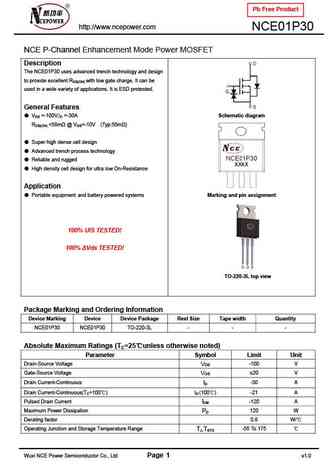
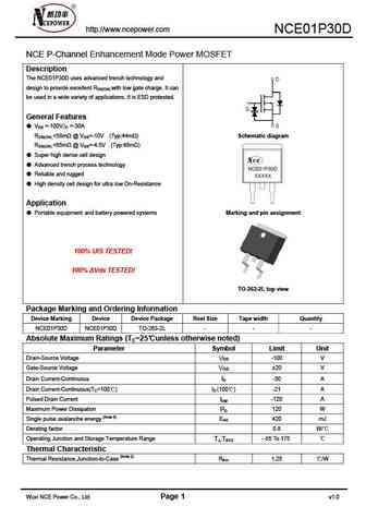
http //www.ncepower.com NCE01P30I NCE P-Channel Enhancement Mode Power MOSFET Description The NCE01P30I uses advanced trench technology and design to provide excellent RDS(ON) with low gate charge. It can be used in a wide variety of applications. It is ESD protested. General Features VDS =-100V,ID =-30A Schematic diagram RDS(ON) ... See More ⇒
nce01p30k.pdf
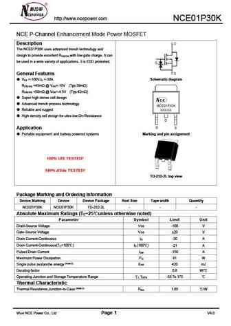
http //www.ncepower.com NCE01P30K NCE P-Channel Enhancement Mode Power MOSFET Description The NCE01P30K uses advanced trench technology and design to provide excellent R with low gate charge. It can DS(ON) be used in a wide variety of applications. It is ESD protested. General Features V =-100V,I =-30A Schematic diagram DS D R ... See More ⇒
nce01p30l.pdf
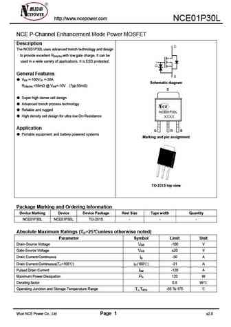
http //www.ncepower.com NCE01P30L NCE P-Channel Enhancement Mode Power MOSFET Description The NCE01P30L uses advanced trench technology and design to provide excellent RDS(ON) with low gate charge. It can be used in a wide variety of applications. It is ESD protested. General Features VDS =-100V,ID =-30A Schematic diagram RDS(ON) ... See More ⇒
Detailed specifications: NCE01H13D, NCE01NP03S, NCE01P05S, NCE01P13, NCE01P13I, NCE01P18, NCE01P18L, NCE01P30D, IRF630, NCE01P30K, NCE01P30L, NCE01P35K, NCE0203S, NCE0205IA, NCE0208IA, NCE0224A, NCE0224AF
Keywords - NCE01P30I MOSFET specs
NCE01P30I cross reference
NCE01P30I equivalent finder
NCE01P30I pdf lookup
NCE01P30I substitution
NCE01P30I replacement
Step-by-step guide to finding a MOSFET replacement. Cross-reference parts and ensure compatibility for your repair or project.
🌐 : EN ES РУ

LIST
Last Update
MOSFET: FTF30P35D | FTF25N35DHVT | FTF15N35D | FTE15C35G | FTP02P15G | FTE02P15G | AKF30N5P0SX | AKF30N10S | AKF20P45D | CM4407
Popular searches
a42 transistor | bc547c | 2sa726 | 2sd313 | 2sc536 | d718 transistor | irfp250n datasheet | 2n5550