NCE3015S Specs and Replacement
Type Designator: NCE3015S
Type of Transistor: MOSFET
Type of Control Channel: N-Channel
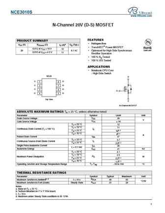
Absolute Maximum Ratings
Pd ⓘ - Maximum Power Dissipation: 3.5 W
|Vds|ⓘ - Maximum Drain-Source Voltage: 30 V
|Vgs|ⓘ - Maximum Gate-Source Voltage: 20 V
|Id| ⓘ - Maximum Drain Current: 15 A
Tj ⓘ - Maximum Junction Temperature: 150 °C
Electrical Characteristics
tr ⓘ - Rise Time: 8 nS
Cossⓘ - Output Capacitance: 205 pF
RDSonⓘ - Maximum Drain-Source On-State Resistance: 0.0095 Ohm
Package: SOP8
NCE3015S substitution
- MOSFET ⓘ Cross-Reference Search
NCE3015S datasheet
nce3015s.pdf
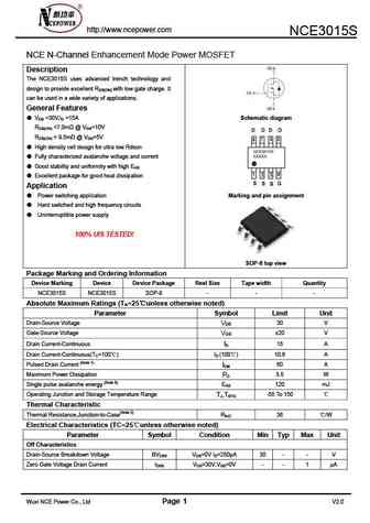
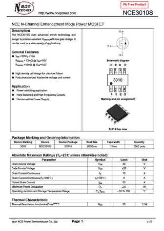
http //www.ncepower.com NCE3015S NCE N-Channel Enhancement Mode Power MOSFET Description The NCE3015S uses advanced trench technology and design to provide excellent RDS(ON) with low gate charge. It can be used in a wide variety of applications. General Features VDS =30V,ID =15A Schematic diagram RDS(ON) ... See More ⇒
nce3013j.pdf
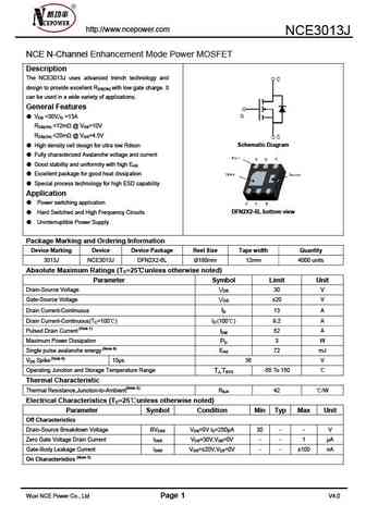
http //www.ncepower.com NCE3013J NCE N-Channel Enhancement Mode Power MOSFET Description The NCE3013J uses advanced trench technology and design to provide excellent RDS(ON) with low gate charge. It can be used in a wide variety of applications. General Features VDS =30V,ID =13A RDS(ON) ... See More ⇒
nce3011e.pdf
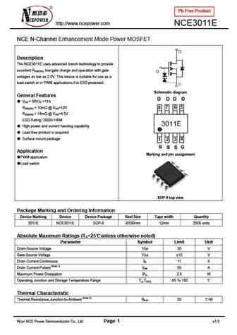
Pb Free Product http //www.ncepower.com NCE3011E NCE N-Channel Enhancement Mode Power MOSFET Description The NCE3011E uses advanced trench technology to provide excellent RDS(ON), low gate charge and operation with gate voltages as low as 2.5V. This device is suitable for use as a load switch or in PWM applications.It is ESD protested. Schematic diagram General Features ... See More ⇒
Detailed specifications: NCE2321, NCE2321A, NCE2323, NCE3008N, NCE3008XM, NCE3008Y, NCE3009S, NCE3013J, IRF640N, NCE3025G, NCE3030K, NCE3030Q, NCE3040Q, NCE3045G, NCE3050I, NCE3050KA, NCE3055
Keywords - NCE3015S MOSFET specs
NCE3015S cross reference
NCE3015S equivalent finder
NCE3015S pdf lookup
NCE3015S substitution
NCE3015S replacement
Can't find your MOSFET? Learn how to find a substitute transistor by analyzing voltage, current and package compatibility
History: 2SJ225
🌐 : EN ES РУ

LIST
Last Update
MOSFET: FTF30P35D | FTF25N35DHVT | FTF15N35D | FTE15C35G | FTP02P15G | FTE02P15G | AKF30N5P0SX | AKF30N10S | AKF20P45D | CM4407
Popular searches
2n5087 equivalent | tip147 datasheet | 2n4124 | mj15022 | toshiba c5198 | irf520n datasheet | tip107 | 2n5457