NCE30P10S Specs and Replacement
Type Designator: NCE30P10S
Type of Transistor: MOSFET
Type of Control Channel: P-Channel
Absolute Maximum Ratings
Pd ⓘ - Maximum Power Dissipation: 3 W
|Vds|ⓘ - Maximum Drain-Source Voltage: 30 V
|Vgs|ⓘ - Maximum Gate-Source Voltage: 20 V
|Id| ⓘ - Maximum Drain Current: 10 A
Tj ⓘ - Maximum Junction Temperature: 150 °C
Electrical Characteristics
tr ⓘ - Rise Time: 9 nS
Cossⓘ - Output Capacitance: 181 pF
RDSonⓘ - Maximum Drain-Source On-State Resistance: 0.034 Ohm
Package: SOP8
NCE30P10S substitution
- MOSFET ⓘ Cross-Reference Search
NCE30P10S datasheet
nce30p10s.pdf
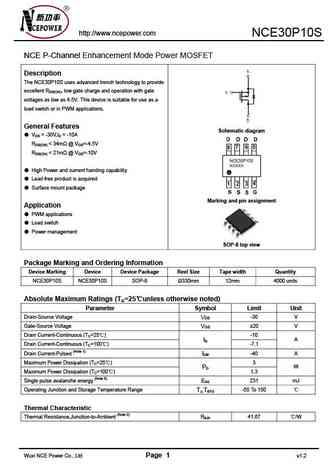
http //www.ncepower.com NCE30P10S NCE P-Channel Enhancement Mode Power MOSFET Description The NCE30P10S uses advanced trench technology to provide excellent RDS(ON), low gate charge and operation with gate voltages as low as 4.5V. This device is suitable for use as a load switch or in PWM applications. General Features Schematic diagram VDS = -30V,ID = -10A RDS(ON) ... See More ⇒
nce30p15s.pdf
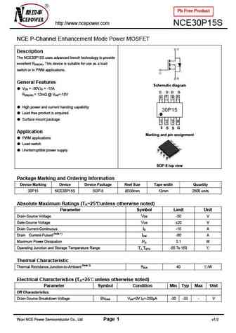
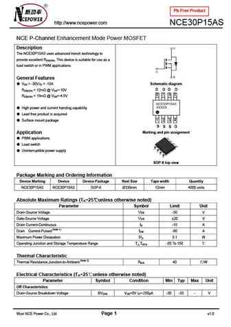
Pb Free Product http //www.ncepower.com NCE30P15S NCE P-Channel Enhancement Mode Power MOSFET Description The NCE30P15S uses advanced trench technology to provide excellent RDS(ON), This device is suitable for use as a load switch or in PWM applications. General Features Schematic diagram VDS = -30V,ID = -15A RDS(ON) ... See More ⇒
nce30p12bs.pdf
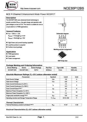
http //www.ncepower.com NCE30P12BS NCE P-Channel Enhancement Mode Power MOSFET Description The NCE30P12BS uses advanced trench technology to provide excellent R , low gate charge and operation with DS(ON) gate voltages as low as 4.5V. This device is suitable for use as a load switch or in PWM applications. General Features V = -30V,I = -12A Schematic diagram DS D R ... See More ⇒
nce30p12s.pdf
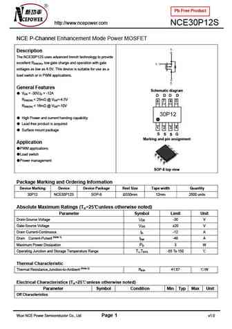
Pb Free Product http //www.ncepower.com NCE30P12S NCE P-Channel Enhancement Mode Power MOSFET Description The NCE30P12S uses advanced trench technology to provide excellent RDS(ON), low gate charge and operation with gate voltages as low as 4.5V. This device is suitable for use as a load switch or in PWM applications. General Features Schematic diagram VDS = -30V,ID = -1... See More ⇒
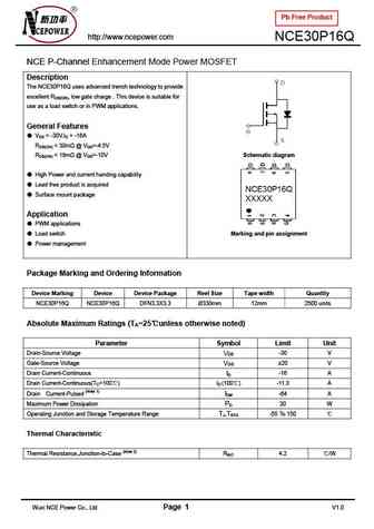
Detailed specifications: NCE30H15BG, NCE30H15BK, NCE30H33LL, NCE30ND35Q, NCE30NP1812G, NCE30NP1812Q, NCE30NP4030G, NCE30P06J, K4145, NCE30P12BS, NCE30P15AS, NCE30P16Q, NCE30P25BQ, NCE30P25Q, NCE30P30L, NCE30P40K, NCE30P55K
Keywords - NCE30P10S MOSFET specs
NCE30P10S cross reference
NCE30P10S equivalent finder
NCE30P10S pdf lookup
NCE30P10S substitution
NCE30P10S replacement
Can't find your MOSFET? Learn how to find a substitute transistor by analyzing voltage, current and package compatibility
🌐 : EN ES РУ

LIST
Last Update
MOSFET: FTF30P35D | FTF25N35DHVT | FTF15N35D | FTE15C35G | FTP02P15G | FTE02P15G | AKF30N5P0SX | AKF30N10S | AKF20P45D | CM4407
Popular searches
bd243 | 2sk170 datasheet | 2n7000 equivalent | tip31 | tip122 transistor | 2sc1079 | 2sc1815 equivalent | 2sa1220