FQD13N06L Specs and Replacement
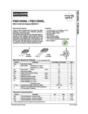
Type Designator: FQD13N06L
Type of Transistor: MOSFET
Type of Control Channel: N-Channel
Absolute Maximum Ratings
Pd ⓘ - Maximum Power Dissipation: 28 W
|Vds|ⓘ - Maximum Drain-Source Voltage: 60 V
|Vgs|ⓘ - Maximum Gate-Source Voltage: 20 V
|Id| ⓘ - Maximum Drain Current: 11 A
Tj ⓘ - Maximum Junction Temperature: 150 °C
Electrical Characteristics
RDSonⓘ - Maximum Drain-Source On-State Resistance: 0.11 Ohm
FQD13N06L substitution
- MOSFET ⓘ Cross-Reference Search
FQD13N06L datasheet
fqd13n06ltf fqd13n06ltm fqd13n06l fqu13n06l fqu13n06ltu.pdf
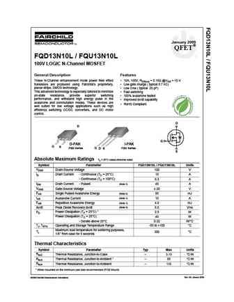
January 2009 QFET FQD13N06L / FQU13N06L 60V LOGIC N-Channel MOSFET General Description Features These N-Channel enhancement mode power field effect 11A, 60V, RDS(on) = 0.115 @VGS = 10 V transistors are produced using Fairchild s proprietary, Low gate charge ( typical 4.8 nC) planar stripe, DMOS technology. Low Crss ( typical 17 pF) This advanced technology has been e... See More ⇒
fqd13n06l fqu13n06l.pdf
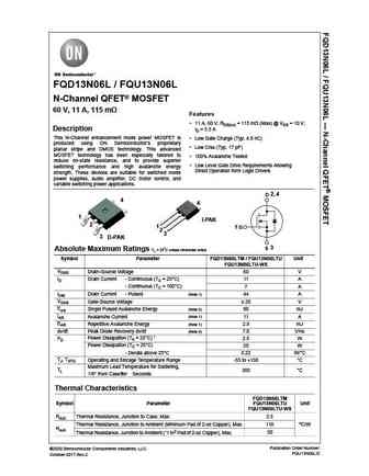
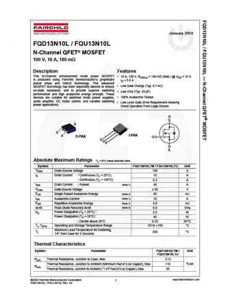
FQD13N06L / FQU13N06L N-Channel QFET MOSFET 60 V, 11 A, 115 m Features 11 A, 60 V, RDS(on) = 115 m (Max) @ VGS = 10 V, Description ID = 5.5 A This N-Channel enhancement mode power MOSFET is Low Gate Charge (Typ. 4.8 nC) produced using ON Semiconductor s proprietary Low Crss (Typ. 17 pF) planar stripe and DMOS technology. This advanced MOSFET technology has b... See More ⇒
fqd13n06tf fqd13n06tm fqd13n06 fqu13n06 fqu13n06tu.pdf
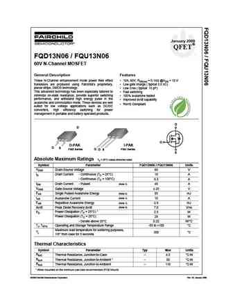
January 2009 QFET FQD13N06 / FQU13N06 60V N-Channel MOSFET General Description Features These N-Channel enhancement mode power field effect 10A, 60V, RDS(on) = 0.14 @VGS = 10 V transistors are produced using Fairchild s proprietary, Low gate charge ( typical 5.8 nC) planar stripe, DMOS technology. Low Crss ( typical 15 pF) This advanced technology has been especially... See More ⇒
fqd13n06.pdf
Is Now Part of To learn more about ON Semiconductor, please visit our website at www.onsemi.com Please note As part of the Fairchild Semiconductor integration, some of the Fairchild orderable part numbers will need to change in order to meet ON Semiconductor s system requirements. Since the ON Semiconductor product management systems do not have the ability to manage part nomenclatur... See More ⇒
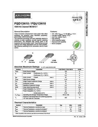
Detailed specifications: FQD12N20, FQP13N50C, FQD12N20L, FQD5N50C, FQD12N20LTMF085, NDS9952A, FQD12P10TMF085, FQD13N06, IRF1010E, FQD13N10, NDS8434, FQD13N10L, MTD3055V, FQD16N25C, FQD17N08L, FQD17P06, FQD18N20V2
Keywords - FQD13N06L MOSFET specs
FQD13N06L cross reference
FQD13N06L equivalent finder
FQD13N06L pdf lookup
FQD13N06L substitution
FQD13N06L replacement
Step-by-step guide to finding a MOSFET replacement. Cross-reference parts and ensure compatibility for your repair or project.
History: SI4848ADY | 4N60KL-TMS4-T | FDMQ8203
🌐 : EN ES РУ
LIST
Last Update
MOSFET: AUB062N08BG | AUB060N08AG | AUB056N10 | AUB056N08BGL | AUB050N085 | AUB050N055 | AUB045N12 | AUB045N10BT | AUB039N10 | AUB034N10
Popular searches
2n5551 | irf540n | irf3205 mosfet | 2n3055 | irfp260n | 2n2222 datasheet | irf9540 | 2n3055 datasheet
