FIR6N70FG Specs and Replacement
Type Designator: FIR6N70FG
Type of Transistor: MOSFET
Type of Control Channel: N-Channel
Absolute Maximum Ratings
Pd ⓘ - Maximum Power Dissipation: 45 W
|Vds|ⓘ - Maximum Drain-Source Voltage: 700 V
|Vgs|ⓘ - Maximum Gate-Source Voltage: 30 V
|Id| ⓘ - Maximum Drain Current: 6 A
Tj ⓘ - Maximum Junction Temperature: 150 °C
Electrical Characteristics
tr ⓘ - Rise Time: 36.93 nS
Cossⓘ - Output Capacitance: 98 pF
RDSonⓘ - Maximum Drain-Source On-State Resistance: 1.7 Ohm
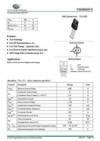
Package: TO-220F
FIR6N70FG substitution
- MOSFET ⓘ Cross-Reference Search
FIR6N70FG datasheet
fir6n70fg.pdf
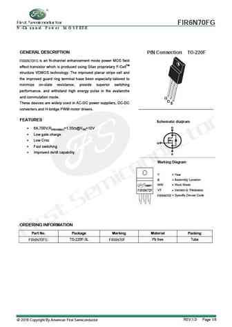
FIR6N70FG N - Ch a n n el P o w e r M O S F ET-E GENERAL DESCRIPTION PIN Connection TO-220F is an N-channel enhancement mode power MOS field FIR6N70FG effect transistor which is produced using Silan proprietary F-CellTM structure VDMOS technology. The improved planar stripe cell and the improved guard ring terminal have been especially tailored to minimize on-state resistance, pr... See More ⇒
fir6n40fg.pdf
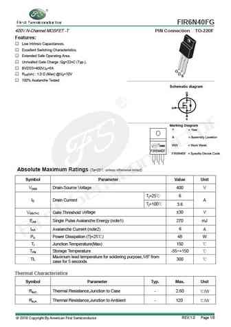
FIR6N40FG 400V N-Channel MOSFET -T PIN Connection TO-220F Features Low Intrinsic Capacitances. Excellent Switching Characteristics. Extended Safe Operating Area. Unrivalled Gate Charge Qg=22nC (Typ.). BVDSS=400V,ID=6A G RDS(on) 1.0 (Max) @VG=10V D S 100% Avalanche Tested g Schematic dia ram D G S Marking Diagram Y = Year A = Assembly... See More ⇒
fir6n90fg.pdf
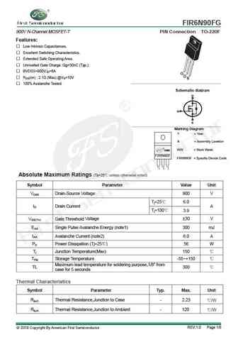
FIR6N90FG 900V N-Channel MOSFET-T PIN Connection TO-220F Features Low Intrinsic Capacitances. Excellent Switching Characteristics. Extended Safe Operating Area. Unrivalled Gate Charge Qg=30nC (Typ.). BVDSS=900V,ID=6A G D S RDS(on) 2.1 (Max) @VG=10V 100% Avalanche Tested g Schematic dia ram D G S Marking Diagram Y = Year A = Assembly L... See More ⇒
Detailed specifications: FIR5N50FG, FIR5N65FG, FIR5N80FG, FIR5NS70ALG, FIR60N04LG, FIR6N40FG, FIR6N60FG, FIR6N65FG, BS170, FIR6N90FG, FIR7NS65AFG, FIR7NS70AFG, FIR7NS70ALG, FIR80N03LG, FIR80N08PG, FIR80N10LG, FIR8N60FG
Keywords - FIR6N70FG MOSFET specs
FIR6N70FG cross reference
FIR6N70FG equivalent finder
FIR6N70FG pdf lookup
FIR6N70FG substitution
FIR6N70FG replacement
Can't find your MOSFET? Learn how to find a substitute transistor by analyzing voltage, current and package compatibility
History: FIR6N90FG
🌐 : EN ES РУ

LIST
Last Update
MOSFET: CM4407 | CM3407 | CM3400 | SVF11N65F | SVF11N65T | FKBB3105 | EHBA036R1 | CRTT067N10N | AP6NA3R2MT | AP65SA145DDT8
Popular searches
6426 mosfet | b1565 | nce82h140 | 2n2369 equivalent | 2sd313 datasheet | k8a50d datasheet | 2sc381 | datasheet mosfet