PP4B10AF Specs and Replacement
Type Designator: PP4B10AF
Type of Transistor: MOSFET
Type of Control Channel: N-Channel
Absolute Maximum Ratings
Pd ⓘ - Maximum Power Dissipation: 60 W
|Vds|ⓘ - Maximum Drain-Source Voltage: 100 V
|Vgs|ⓘ - Maximum Gate-Source Voltage: 20 V
|Id| ⓘ - Maximum Drain Current: 79 A
Tj ⓘ - Maximum Junction Temperature: 175 °C
Electrical Characteristics
tr ⓘ - Rise Time: 58 nS
Cossⓘ - Output Capacitance: 757 pF
RDSonⓘ - Maximum Drain-Source On-State Resistance: 0.0044 Ohm
Package: TO-220F
PP4B10AF substitution
- MOSFET ⓘ Cross-Reference Search
PP4B10AF datasheet
pp4b10af.pdf
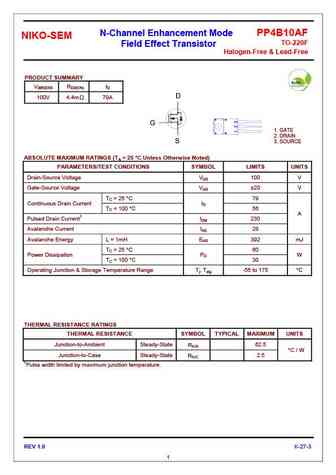
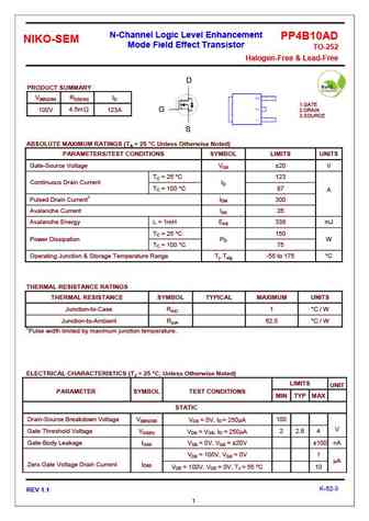
N-Channel Enhancement Mode PP4B10AF NIKO-SEM TO-220F Field Effect Transistor Halogen-Free & Lead-Free PRODUCT SUMMARY V(BR)DSS RDS(ON) ID D 100V 4.4m 79A G 1. GATE 2. DRAIN S 3. SOURCE ABSOLUTE MAXIMUM RATINGS (TA = 25 C Unless Otherwise Noted) PARAMETERS/TEST CONDITIONS SYMBOL LIMITS UNITS Drain-Source Voltage VDS 100 V Gate-Source Voltage VGS 20 V TC = ... See More ⇒
pp4b10ak.pdf
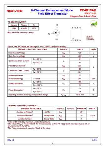
N-Channel Enhancement Mode PP4B10AK NIKO-SEM PDFN 5x6P Field Effect Transistor Halogen-Free & Lead-Free PRODUCT SUMMARY V(BR)DSS RDS(ON) ID D D D D D 100V 4.2m 127A MSL (Moisture Sensitivity Level) 1. G G. GATE D. DRAIN S S. SOURCE #1 S S S G ABSOLUTE MAXIMUM RATINGS (TA = 25 C Unless Otherwise Noted) PARAMETERS/TEST CONDITIONS SYMBOL LIMITS UNITS Drain-So... See More ⇒
pp4b10as.pdf
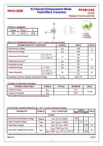
N-Channel Enhancement Mode PP4B10AS NIKO-SEM Field Effect Transistor TO-263 Halogen-Free & Lead-Free D PRODUCT SUMMARY V(BR)DSS RDS(ON) ID G 100V 4.4m 139A 1. GATE 2. DRAIN 3. SOURCE S ABSOLUTE MAXIMUM RATINGS (TA = 25 C Unless Otherwise Noted) PARAMETERS/TEST CONDITIONS SYMBOL LIMITS UNITS Drain-Source Voltage VDS 100 V Gate-Source Voltage VGS 20 V T... See More ⇒
pp4b10at.pdf
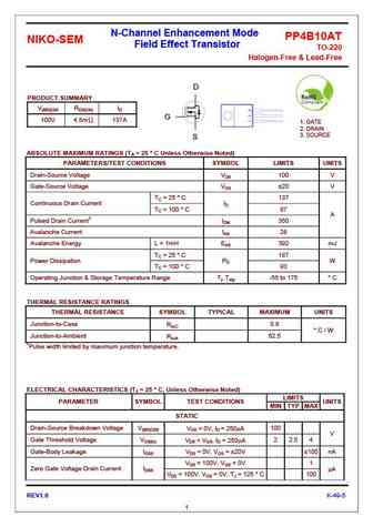
N-Channel Enhancement Mode PP4B10AT NIKO-SEM Field Effect Transistor TO-220 Halogen-Free & Lead-Free D PRODUCT SUMMARY V(BR)DSS RDS(ON) ID G 100V 4.5m 137A 1. GATE 2. DRAIN 3. SOURCE S ABSOLUTE MAXIMUM RATINGS (TA = 25 C Unless Otherwise Noted) PARAMETERS/TEST CONDITIONS SYMBOL LIMITS UNITS Drain-Source Voltage VDS 100 V Gate-Source Voltage VGS 20 V T... See More ⇒
Detailed specifications: PP2G10AT, PP2H06AK, PP2H06AT, PP2H06BK, PP4515BD, PP4515BK, PP4515BL, PP4B10AD, IRFP064N, PP4B10AK, PP4B10AS, PP4B10AT, PP4B10BD, PP4B10BF, PP4B10BK, PP4B10BS, PP9C15AD
Keywords - PP4B10AF MOSFET specs
PP4B10AF cross reference
PP4B10AF equivalent finder
PP4B10AF pdf lookup
PP4B10AF substitution
PP4B10AF replacement
Need a MOSFET replacement? Our guide shows you how to find a perfect substitute by comparing key parameters and specs
🌐 : EN ES РУ

LIST
Last Update
MOSFET: AUW033N08BG | AUW025N10 | AUR030N10 | AUR020N10 | AUR020N085 | AUR014N10 | AUP074N10 | AUP065N10 | AUP062N08BG | AUP060N08AG
Popular searches
se9302 transistor | fr5305 datasheet | y2 transistor | 40n06 | bc108b | oc84 | c6090 | ksa1015yta