PP9C15AT Specs and Replacement
Type Designator: PP9C15AT
Type of Transistor: MOSFET
Type of Control Channel: N-Channel
Absolute Maximum Ratings
Pd ⓘ - Maximum Power Dissipation: 188 W
|Vds|ⓘ - Maximum Drain-Source Voltage: 150 V
|Vgs|ⓘ - Maximum Gate-Source Voltage: 20 V
|Id| ⓘ - Maximum Drain Current: 89 A
Tj ⓘ - Maximum Junction Temperature: 175 °C
Electrical Characteristics
tr ⓘ - Rise Time: 47 nS
Cossⓘ - Output Capacitance: 326 pF
RDSonⓘ - Maximum Drain-Source On-State Resistance: 0.0093 Ohm
Package: TO-220
PP9C15AT substitution
- MOSFET ⓘ Cross-Reference Search
PP9C15AT datasheet
pp9c15at.pdf
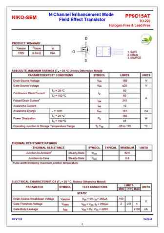
N-Channel Enhancement Mode PP9C15AT NIKO-SEM Field Effect Transistor TO-220 Halogen-Free & Lead-Free D PRODUCT SUMMARY V(BR)DSS RDS(ON) ID G 1. GATE 150V 9.3m 89A 2. DRAIN 3. SOURCE S ABSOLUTE MAXIMUM RATINGS (TA = 25 C Unless Otherwise Noted) PARAMETERS/TEST CONDITIONS SYMBOL LIMITS UNITS Drain-Source Voltage VDS 150 V Gate-Source Voltage VGS 20 V TC = ... See More ⇒
pp9c15af.pdf
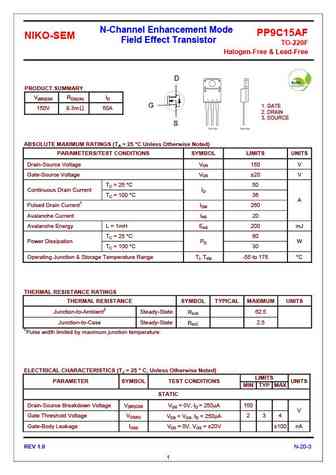
N-Channel Enhancement Mode PP9C15AF NIKO-SEM Field Effect Transistor TO-220F Halogen-Free & Lead-Free D PRODUCT SUMMARY V(BR)DSS RDS(ON) ID G 1. GATE 150V 9.3m 50A 2. DRAIN 3. SOURCE S ABSOLUTE MAXIMUM RATINGS (TA = 25 C Unless Otherwise Noted) PARAMETERS/TEST CONDITIONS SYMBOL LIMITS UNITS Drain-Source Voltage VDS 150 V Gate-Source Voltage VGS 20 V TC =... See More ⇒
pp9c15ak.pdf
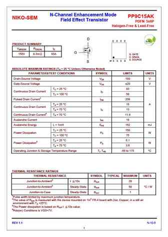
N-Channel Enhancement Mode PP9C15AK NIKO-SEM Field Effect Transistor PDFN 5x6P Halogen-Free & Lead-Free D D D D D PRODUCT SUMMARY V(BR)DSS RDS(ON) ID G 150V 9.3m 83A G. GATE D. DRAIN S. SOURCE #1 S S S G S ABSOLUTE MAXIMUM RATINGS (TA = 25 C Unless Otherwise Noted) PARAMETERS/TEST CONDITIONS SYMBOL LIMITS UNITS Drain-Source Voltage VDS 150 V Gate-Source ... See More ⇒
pp9c15ad.pdf

N-Channel Enhancement Mode PP9C15AD NIKO-SEM Field Effect Transistor TO-252 Halogen-Free & Lead-Free D PRODUCT SUMMARY V(BR)DSS RDS(ON) ID G 1. GATE 150V 9.3m 70A 2. DRAIN 3. SOURCE S ABSOLUTE MAXIMUM RATINGS (TA = 25 C Unless Otherwise Noted) PARAMETERS/TEST CONDITIONS SYMBOL LIMITS UNITS Drain-Source Voltage VDS 150 V Gate-Source Voltage VGS 20 V TC = ... See More ⇒
Detailed specifications: PP4B10AT, PP4B10BD, PP4B10BF, PP4B10BK, PP4B10BS, PP9C15AD, PP9C15AF, PP9C15AK, IRFP460, PP9H06BD, PP9H06BEA, PP9H06BI, PP9H06BK, PP9H06BV, PQ5G4JN, PQ5U2JN, PQ6S2JN
Keywords - PP9C15AT MOSFET specs
PP9C15AT cross reference
PP9C15AT equivalent finder
PP9C15AT pdf lookup
PP9C15AT substitution
PP9C15AT replacement
Learn how to find the right MOSFET substitute. A guide to cross-reference, check specs and replace MOSFETs in your circuits.
History: PP4B10BK
🌐 : EN ES РУ

LIST
Last Update
MOSFET: AUW033N08BG | AUW025N10 | AUR030N10 | AUR020N10 | AUR020N085 | AUR014N10 | AUP074N10 | AUP065N10 | AUP062N08BG | AUP060N08AG
Popular searches
pk6d0ba mosfet | 2sd726 | c536 transistor equivalent | 2sa1294 datasheet | mp10b transistor | bc182b | 2n3054 transistor equivalent | 2n554