AOW125A60 Specs and Replacement
Type Designator: AOW125A60
Type of Transistor: MOSFET
Type of Control Channel: N-Channel
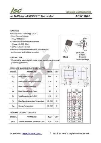
Absolute Maximum Ratings
Pd ⓘ - Maximum Power Dissipation: 312.5 W
|Vds|ⓘ - Maximum Drain-Source Voltage: 600 V
|Vgs|ⓘ - Maximum Gate-Source Voltage: 20 V
|Id| ⓘ - Maximum Drain Current: 28 A
Tj ⓘ - Maximum Junction Temperature: 150 °C
Electrical Characteristics
tr ⓘ - Rise Time: 34 nS
Cossⓘ - Output Capacitance: 85 pF
RDSonⓘ - Maximum Drain-Source On-State Resistance: 0.125 Ohm
Package: TO262
AOW125A60 substitution
- MOSFET ⓘ Cross-Reference Search
AOW125A60 datasheet
aow125a60.pdf
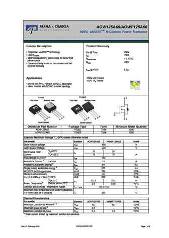
AOW125A60/AOWF125A60 TM 600V, a MOS5 N-Channel Power Transistor General Description Product Summary VDS @ Tj,max 700V Proprietary aMOS5TM technology Low RDS(ON) IDM 100A Optimized switching parameters for better EMI RDS(ON),max ... See More ⇒
aow125a60 aowf125a60.pdf

AOW125A60/AOWF125A60 TM 600V, a MOS5 N-Channel Power Transistor General Description Product Summary VDS @ Tj,max 700V Proprietary aMOS5TM technology Low RDS(ON) IDM 100A Optimized switching parameters for better EMI RDS(ON),max ... See More ⇒
aow12n60 aowf12n60.pdf
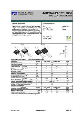
AOW12N60/AOWF12N60 600V,12A N-Channel MOSFET General Description Product Summary VDS 700V@150 The AOW12N60 & AOWF12N60 have been fabricated using an advanced high voltage MOSFET process that is ID (at VGS=10V) 12A designed to deliver high levels of performance and RDS(ON) (at VGS=10V) ... See More ⇒
aow12n50.pdf
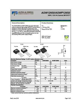
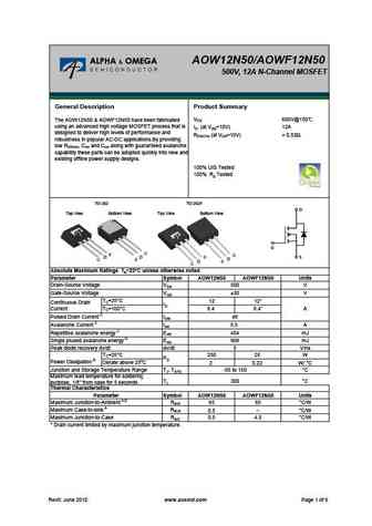
AOW12N50/AOWF12N50 500V, 12A N-Channel MOSFET General Description Product Summary VDS The AOW12N50 & AOWF12N50 have been fabricated 600V@150 12A using an advanced high voltage MOSFET process that is ID (at VGS=10V) designed to deliver high levels of performance and ... See More ⇒

Detailed specifications: AOD66620, AOD66643, AOD66919, AOD66920, AOD66923, AOD780A70, AOD950A70, AOD609G, IRFZ46N, AOW190A60C, AOW360A70, AOW66613, AOW66616, AOWF095A60, AOWF125A60, AOWF160A60, AOWF190A60C
Keywords - AOW125A60 MOSFET specs
AOW125A60 cross reference
AOW125A60 equivalent finder
AOW125A60 pdf lookup
AOW125A60 substitution
AOW125A60 replacement
Learn how to find the right MOSFET substitute. A guide to cross-reference, check specs and replace MOSFETs in your circuits.
🌐 : EN ES РУ

LIST
Last Update
MOSFET: AKF30N5P0SX | AKF30N10S | AKF20P45D | CM4407 | CM3407 | CM3400 | SVF11N65F | SVF11N65T | FKBB3105 | EHBA036R1
Popular searches
c5198 transistor | ru7088r | 2sa733 replacement | 2n3906 transistor equivalent | 2sc4883 | tip31a datasheet | d882 datasheet | tip29 transistor