FQPF6N90C Specs and Replacement
Type Designator: FQPF6N90C
Type of Transistor: MOSFET
Type of Control Channel: N-Channel
Absolute Maximum Ratings
Pd ⓘ
- Maximum Power Dissipation: 56 W
|Vds|ⓘ - Maximum Drain-Source Voltage: 900 V
|Vgs|ⓘ - Maximum Gate-Source Voltage: 30 V
|Id| ⓘ - Maximum Drain Current: 6 A
Tj ⓘ - Maximum Junction Temperature: 150 °C
Electrical Characteristics
RDSonⓘ - Maximum Drain-Source On-State Resistance: 2.3 Ohm
Package: TO220F
- MOSFET ⓘ Cross-Reference Search
FQPF6N90C datasheet
..1. Size:860K fairchild semi
fqp6n90c fqpf6n90c.pdf 

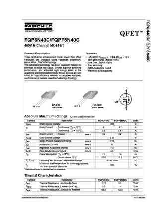
TM QFET FQP6N90C/FQPF6N90C 900V N-Channel MOSFET General Description Features These N-Channel enhancement mode power field effect 6A, 900V, RDS(on) = 2.3 @VGS = 10 V transistors are produced using Fairchild s proprietary, Low gate charge ( typical 30 nC) planar stripe, DMOS technology. Low Crss ( typical 11 pF) This advanced technology has been especially tailored to ... See More ⇒
..2. Size:1255K onsemi
fqp6n90c fqpf6n90c.pdf

Is Now Part of To learn more about ON Semiconductor, please visit our website at www.onsemi.com Please note As part of the Fairchild Semiconductor integration, some of the Fairchild orderable part numbers will need to change in order to meet ON Semiconductor s system requirements. Since the ON Semiconductor product management systems do not have the ability to manage part nomenclatur... See More ⇒
0.1. Size:858K fairchild semi
fqpf6n90ct.pdf

TM QFET FQP6N90C/FQPF6N90C 900V N-Channel MOSFET General Description Features These N-Channel enhancement mode power field effect 6A, 900V, RDS(on) = 2.3 @VGS = 10 V transistors are produced using Fairchild s proprietary, Low gate charge ( typical 30 nC) planar stripe, DMOS technology. Low Crss ( typical 11 pF) This advanced technology has been especially tailored to ... See More ⇒
6.1. Size:600K fairchild semi
fqpf6n90.pdf
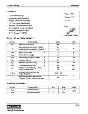
QFET N-CHANNEL FQPF6N90 FEATURES BVDSS = 900V Advanced New Design RDS(ON) = 1.9 Avalanche Rugged Technology ID = 3.4A Rugged Gate Oxide Technology Very Low Intrinsic Capacitances Excellent Switching Characteristics TO-220F Unrivalled Gate Charge 40nC (Typ.) Extended Safe Operating Area Lower RDS(ON) 1.5 (Typ.) 1 2 3 1. Gate 2. Drain 3. Sou... See More ⇒
8.1. Size:733K fairchild semi
fqpf6n15.pdf
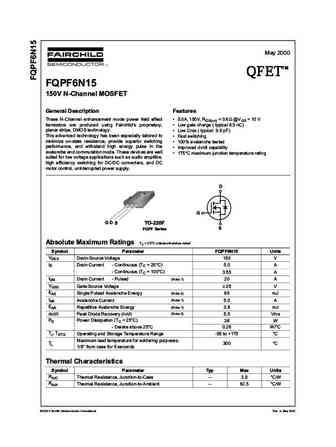
May 2000 TM QFET QFET QFET QFET 150V N-ChanneI MOSFET GeneraI Description Features These N-Channel enhancement mode power field effect 5.0A, 150V, RDS(on) = 0.6 @VGS = 10 V transistors are produced using Fairchild s proprietary, Low gate charge ( typical 6.5 nC) planar stripe, DMOS technology. Low Crss ( typical 9.6 pF) This advanced technology has been e... See More ⇒
8.3. Size:1088K fairchild semi
fqp6n40cf fqpf6n40cf.pdf
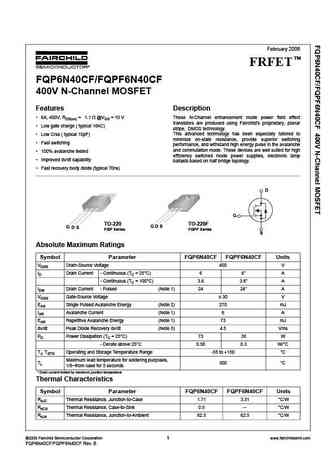
February 2006 TM FRFET FQP6N40CF/FQPF6N40CF 400V N-Channel MOSFET Features Description 6A, 400V, RDS(on) = 1.1 @VGS = 10 V These N-Channel enhancement mode power field effect transistors are produced using Fairchild s proprietary, planar Low gate charge ( typical 16nC) stripe, DMOS technology. This advanced technology has been especially tailored to Low Crss ( typi... See More ⇒
8.4. Size:542K fairchild semi
fqpf6n60.pdf
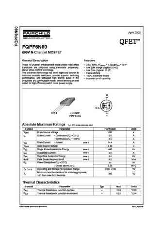
April 2000 TM QFET QFET QFET QFET FQPF6N60 600V N-Channel MOSFET General Description Features These N-Channel enhancement mode power field effect 3.6A, 600V, RDS(on) = 1.5 @VGS = 10 V transistors are produced using Fairchild s proprietary, Low gate charge ( typical 20 nC) planar stripe, DMOS technology. Low Crss ( typical 10 pF) This advanced technology has been es... See More ⇒
8.5. Size:664K fairchild semi
fqpf6n80.pdf
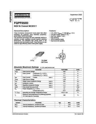
September 2000 TM QFET FQPF6N80 800V N-Channel MOSFET General Description Features These N-Channel enhancement mode power field effect 3.3A, 800V, RDS(on) = 1.95 @VGS = 10 V transistors are produced using Fairchild s proprietary, Low gate charge ( typical 31 nC) planar stripe, DMOS technology. Low Crss ( typical 14 pF) This advanced technology has been especially tail... See More ⇒
8.6. Size:758K fairchild semi
fqpf6n50.pdf

April 2000 TM QFET QFET QFET QFET 500V N-ChanneI MOSFET GeneraI Description Features These N-Channel enhancement mode power field effect 3.6A, 500V, RDS(on) = 1.3 @VGS = 10 V transistors are produced using Fairchild s proprietary, Low gate charge ( typical 17 nC) planar stripe, DMOS technology. Low Crss ( typical 11 pF) This advanced technology has been ... See More ⇒
8.7. Size:931K fairchild semi
fqp6n60c fqp6n60c fqpf6n60c fqpf6n60c.pdf
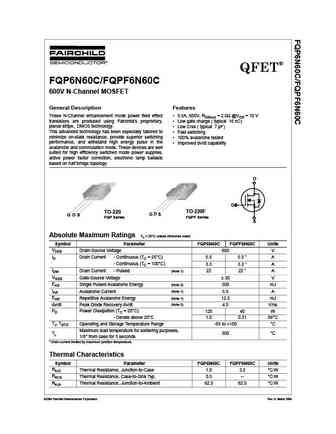
QFET FQP6N60C/FQPF6N60C 600V N-Channel MOSFET General Description Features These N-Channel enhancement mode power field effect 5.5A, 600V, RDS(on) = 2.0 @VGS = 10 V transistors are produced using Fairchild s proprietary, Low gate charge ( typical 16 nC) planar stripe, DMOS technology. Low Crss ( typical 7 pF) This advanced technology has been especially tailored to ... See More ⇒
8.8. Size:558K fairchild semi
fqpf6n70.pdf
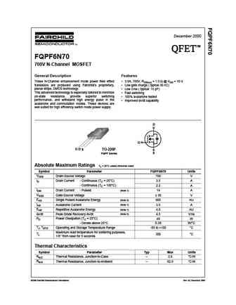
December 2000 TM QFET QFET QFET QFET FQPF6N70 700V N-Channel MOSFET General Description Features These N-Channel enhancement mode power field effect 3.5A, 700V, RDS(on) = 1.5 @ VGS = 10 V transistors are produced using Fairchild s proprietary, Low gate charge ( typical 30 nC) planar stripe, DMOS technology. Low Crss ( typical 15 pF) This advanced technology is esp... See More ⇒
8.9. Size:723K fairchild semi
fqpf6n25.pdf
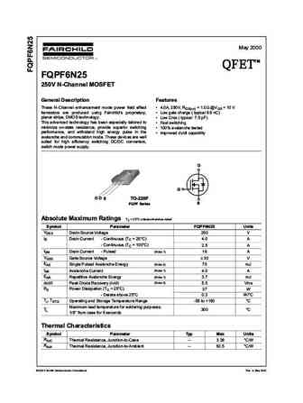
May 2000 TM QFET QFET QFET QFET 250V N-ChanneI MOSFET GeneraI Description Features These N-Channel enhancement mode power field effect 4.0A, 250V, RDS(on) = 1.0 @VGS = 10 V transistors are produced using Fairchild s proprietary, Low gate charge ( typical 6.6 nC) planar stripe, DMOS technology. Low Crss ( typical 7.5 pF) This advanced technology has been e... See More ⇒
8.10. Size:1001K fairchild semi
fqpf6n80t.pdf
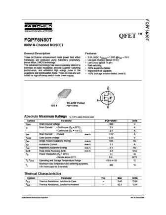
TM QFET FQPF6N80T 800V N-Channel MOSFET General Description Features These N-Channel enhancement mode power field effect 3.3A, 800V, RDS(on) = 1.95 @VGS = 10 V transistors are produced using Fairchild s proprietary, Low gate charge ( typical 31 nC) planar stripe, DMOS technology. Low Crss ( typical 14 pF) This advanced technology has been especially tailored to ... See More ⇒
8.11. Size:889K fairchild semi
fqp6n80c fqpf6n80c.pdf
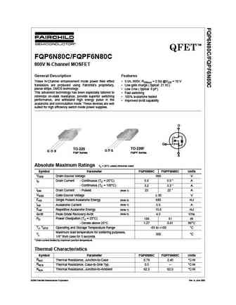
TM QFET FQP6N80C/FQPF6N80C 800V N-Channel MOSFET General Description Features These N-Channel enhancement mode power field effect 5.5A, 800V, RDS(on) = 2.5 @VGS = 10 V transistors are produced using Fairchild s proprietary, Low gate charge ( typical 21 nC) planar stripe, DMOS technology. Low Crss ( typical 8 pF) This advanced technology has been especially tailored to ... See More ⇒
8.13. Size:1046K onsemi
fqp6n60c fqpf6n60c.pdf

Is Now Part of To learn more about ON Semiconductor, please visit our website at www.onsemi.com Please note As part of the Fairchild Semiconductor integration, some of the Fairchild orderable part numbers will need to change in order to meet ON Semiconductor s system requirements. Since the ON Semiconductor product management systems do not have the ability to manage part nomenclatur... See More ⇒
8.14. Size:549K onsemi
fqpf6n80t.pdf

Is Now Part of To learn more about ON Semiconductor, please visit our website at www.onsemi.com Please note As part of the Fairchild Semiconductor integration, some of the Fairchild orderable part numbers will need to change in order to meet ON Semiconductor s system requirements. Since the ON Semiconductor product management systems do not have the ability to manage part nomenclatur... See More ⇒
8.15. Size:890K onsemi
fqp6n80c fqpf6n80c.pdf

TM QFET FQP6N80C/FQPF6N80C 800V N-Channel MOSFET General Description Features These N-Channel enhancement mode power field effect 5.5A, 800V, RDS(on) = 2.5 @VGS = 10 V transistors are produced using Fairchild s proprietary, Low gate charge ( typical 21 nC) planar stripe, DMOS technology. Low Crss ( typical 8 pF) This advanced technology has been especially tailored to ... See More ⇒
8.16. Size:921K cn vbsemi
fqpf6n60c.pdf
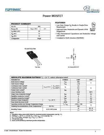
FQPF6N60C www.VBsemi.tw Power MOSFET FEATURES PRODUCT SUMMARY Low Gate Charge Qg Results in Simple Drive VDS (V) 650 Available Requirement RDS(on) ( )VGS = 10 V 2.1 RoHS* Improved Gate, Avalanche and Dynamic dV/dt COMPLIANT Qg (Max.) (nC) 48 Ruggedness Qgs (nC) 12 Fully Characterized Capacitance and Avalanche Voltage and Current Qgd (nC) 19 Compliant to RoHS ... See More ⇒
Detailed specifications: FQPF5P20
, FQPF630
, FDMC8296
, FQPF65N06
, FQPF6N80C
, FDMS8880
, FQPF6N80T
, FDH50N50
, 10N65
, FQPF70N10
, FDH45N50F
, FQPF7N60
, FDN5632NF085
, FQPF7N65C
, FQPF7N80C
, FDD16AN08F085
, FQPF7P20
.
History: FDH45N50F
| FQPF70N10
Keywords - FQPF6N90C MOSFET specs
FQPF6N90C cross reference
FQPF6N90C equivalent finder
FQPF6N90C pdf lookup
FQPF6N90C substitution
FQPF6N90C replacement
Step-by-step guide to finding a MOSFET replacement. Cross-reference parts and ensure compatibility for your repair or project.