23N50D Datasheet. Specs and Replacement
Type Designator: 23N50D 📄📄
Type of Transistor: MOSFET
Type of Control Channel: N-Channel
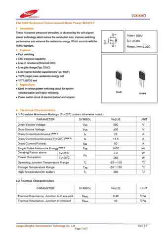
Absolute Maximum Ratings
Pd ⓘ - Maximum Power Dissipation: 260 W
|Vds|ⓘ - Maximum Drain-Source Voltage: 500 V
|Vgs|ⓘ - Maximum Gate-Source Voltage: 30 V
|Id| ⓘ - Maximum Drain Current: 23 A
Tj ⓘ - Maximum Junction Temperature: 150 °C
Electrical Characteristics
tr ⓘ - Rise Time: 65 nS
Cossⓘ - Output Capacitance: 277 pF
RDSonⓘ - Maximum Drain-Source On-State Resistance: 0.28 Ohm
Package: TO3P
TO3PN
📄📄 Copy
- MOSFET ⓘ Cross-Reference Search
23N50D datasheet
..1. Size:1488K cn wxdh
23n50d.pdf 
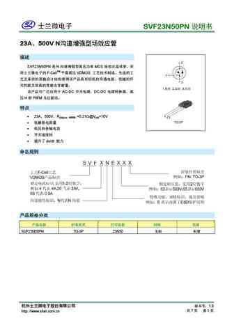
23N50D 23A 500V N-channel Enhancement Mode Power MOSFET 1 Description These N-channel enhanced vdmosfets, is obtained by the self-aligned V DSS = 500V planar technology which reduce the conduction loss, improve switching I = 23.0A D performance and enhance the avalanche energy. Which accords with the RoHS standard. R DS(on) TYP) =0.22 2 Features Fast switching ESD im... See More ⇒
0.1. Size:837K magnachip
mdq23n50dtp.pdf
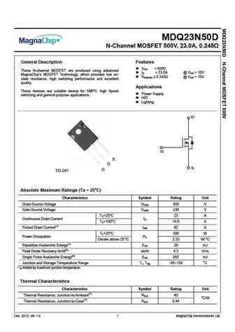
MDQ23N50D N-Channel MOSFET 500V, 23.0A, 0.245 General Description Features . VDS = 500V These N-channel MOSFET are produced using advanced ID = 23.0A @ VGS = 10V MagnaChip s MOSFET Technology, which provides low on- RDS(ON) 0.245 @ VGS = 10V state resistance, high switching performance and excellent quality. Applications These devices are suitable device fo... See More ⇒
0.2. Size:328K inchange semiconductor
mdq23n50dtp.pdf
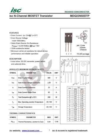
isc N-Channel MOSFET Transistor MDQ23N50DTP FEATURES Drain Current I = 23A@ T =25 D C Drain Source Voltage V = 500V(Min) DSS Static Drain-Source On-Resistance R = 0.245 (Max) @V = 10V DS(on) GS 100% avalanche tested Minimum Lot-to-Lot variations for robust device performance and reliable operation DESCRIPTION motor drive, DC-DC converter, power switch and so... See More ⇒
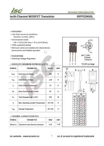
9.1. Size:104K international rectifier
irfp23n50l.pdf
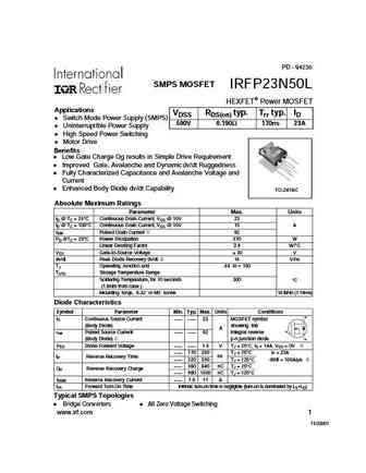
PD - 94230 SMPS MOSFET IRFP23N50L HEXFET Power MOSFET Applications VDSS RDS(on) typ. Trr typ. ID Switch Mode Power Supply (SMPS) 500V 0.190 170ns 23A UninterruptIble Power Supply High Speed Power Switching Motor Drive Benefits Low Gate Charge Qg results in Simple Drive Requirement Improved Gate, Avalanche and Dynamicdv/dt Ruggedness Fully Characterized Capacitance and ... See More ⇒
9.2. Size:606K rohm
rdd023n50.pdf
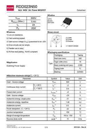
RDD023N50 Nch 500V 2A Power MOSFET Datasheet lOutline VDSS 500V CPT3 (SC-63) RDS(on) (Max.) 5.4W (SOT-428) ID 2A (1) (2) (3) PD 20W lFeatures lInner circuit 1) Low on-resistance. (1) Gate 2) Fast switching speed. (2) Drain (3) Source 3) Gate-source voltage (VGSS) guaranteed to be 30V. 4) Drive circuits can be simple. *1 BODY DIODE 5) Parallel use is easy. ... See More ⇒
9.3. Size:188K vishay
irfp23n50l sihfp23n50l.pdf

IRFP23N50L, SiHFP23N50L Vishay Siliconix Power MOSFET FEATURES PRODUCT SUMMARY Superfast Body Diode Eliminates the Need for VDS (V) 500 External Diodes in ZVS Applications Available RDS(on) ( )VGS = 10 V 0.190 Lower Gate Charge Results in Simpler Drive RoHS* Qg (Max.) (nC) 150 COMPLIANT Requirements Qgs (nC) 44 Enhanced dV/dt Capabilities Offer Improved Ruggedness ... See More ⇒
9.4. Size:192K vishay
irfp23n50l irfp23n50lpbf sihfp23n50l.pdf
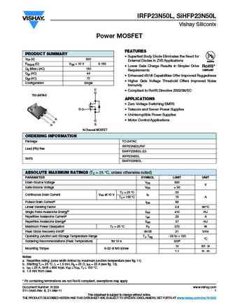
IRFP23N50L, SiHFP23N50L Vishay Siliconix Power MOSFET FEATURES PRODUCT SUMMARY Superfast Body Diode Eliminates the Need for VDS (V) 500 External Diodes in ZVS Applications Available RDS(on) ( )VGS = 10 V 0.190 Lower Gate Charge Results in Simpler Drive RoHS* Qg (Max.) (nC) 150 COMPLIANT Requirements Qgs (nC) 44 Enhanced dV/dt Capabilities Offer Improved Ruggedness ... See More ⇒
9.5. Size:490K fuji
fmv23n50es.pdf
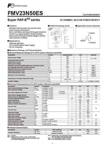
FMV23N50ES FUJI POWER MOSFET Super FAP-E3S series N-CHANNEL SILICON POWER MOSFET Features Outline Drawings [mm] Equivalent circuit schematic Maintains both low power loss and low noise TO-220F (SLS) Lower R (on) characteristic DS More controllable switching dv/dt by gate resistance Drain(D) Smaller V ringing waveform during switching GS Narrow band of the gate threshold voltage (4.2... See More ⇒
9.6. Size:406K fuji
fmv23n50e.pdf
FMV23N50E FUJI POWER MOSFET Super FAP-E3 series N-CHANNEL SILICON POWER MOSFET Features Outline Drawings [mm] Equivalent circuit schematic Maintains both low power loss and low noise TO-220F(SLS) Lower R (on) characteristic DS More controllable switching dv/dt by gate resistance Drain(D) Smaller V ringing waveform during switching GS Narrow band of the gate threshold voltage (3.0 0.... See More ⇒
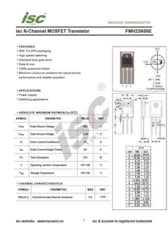
9.7. Size:504K fuji
fmh23n50es.pdf
FMH23N50ES FUJI POWER MOSFET Super FAP-E3S series N-CHANNEL SILICON POWER MOSFET Features Outline Drawings [mm] Equivalent circuit schematic Maintains both low power loss and low noise TO-3P (Q) Lower R (on) characteristic DS More controllable switching dv/dt by gate resistance Drain(D) Smaller V ringing waveform during switching GS Narrow band of the gate threshold voltage (4.2 0.5... See More ⇒
9.8. Size:435K fuji
fmr23n50e.pdf
FMR23N50E FUJI POWER MOSFET Super FAP-E3 series N-CHANNEL SILICON POWER MOSFET Features Outline Drawings [mm] Equivalent circuit schematic Maintains both low power loss and low noise TO-3PF Lower R (on) characteristic DS More controllable switching dv/dt by gate resistance Drain(D) Smaller V ringing waveform during switching GS Narrow band of the gate threshold voltage (3.0 0.5V) H... See More ⇒
9.9. Size:496K fuji
fmr23n50es.pdf

FMR23N50ES FUJI POWER MOSFET Super FAP-E3S series N-CHANNEL SILICON POWER MOSFET Features Outline Drawings [mm] Equivalent circuit schematic Maintains both low power loss and low noise TO-3PF Lower R (on) characteristic DS More controllable switching dv/dt by gate resistance Drain(D) Smaller V ringing waveform during switching GS Narrow band of the gate threshold voltage (4.2 0.5V) ... See More ⇒
9.10. Size:448K fuji
fmh23n50e.pdf
FMH23N50E FUJI POWER MOSFET Super FAP-E3 series N-CHANNEL SILICON POWER MOSFET Features Outline Drawings [mm] Equivalent circuit schematic Maintains both low power loss and low noise TO-3P(Q) Lower R (on) characteristic DS More controllable switching dv/dt by gate resistance Drain(D) Smaller V ringing waveform during switching GS Narrow band of the gate threshold voltage (3.0 0.5V) ... See More ⇒
9.11. Size:335K taiwansemi
tsm23n50cn.pdf
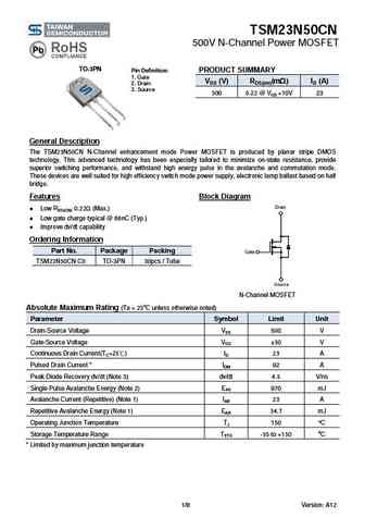
TSM23N50CN 500V N-Channel Power MOSFET TO-3PN Pin Definition PRODUCT SUMMARY 1. Gate VDS (V) RDS(on)(m ) ID (A) 2. Drain 3. Source 500 0.22 @ VGS =10V 23 General Description The TSM23N50CN N-Channel enhancement mode Power MOSFET is produced by planar stripe DMOS technology. This advanced technology has been especially tailored to minimize on-state resistance, provide ... See More ⇒
9.13. Size:720K belling
bl23n50-p bl23n50-a bl23n50-w bl23n50-k.pdf
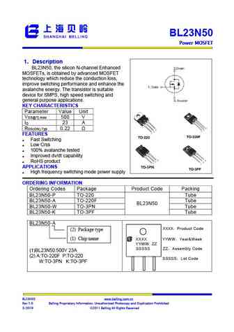
BL23N50 Power MOSFET Power MOSFET Power MOSFET Power MOSFET 1 Description BL23N50, the silicon N-channel Enhanced MOSFETs, is obtained by advanced MOSFET technology which reduce the conduction loss, improve switching performance and enhance the avalanche energy. The transistor is suitable device for SMPS, high speed switching and general purpose applicati... See More ⇒
9.14. Size:494K trinnotech
tman23n50a.pdf

TMAN23N50A N-channel MOSFET Features BVDSS ID RDS(on) Low gate charge 500V 23A ... See More ⇒
9.15. Size:508K trinnotech
tman23n50.pdf
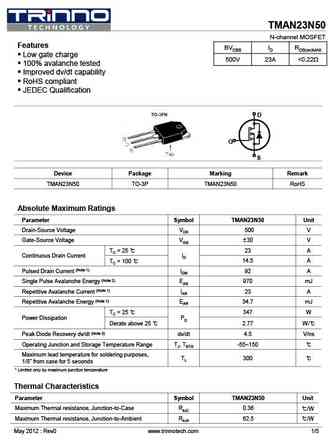
TMAN23N50 N-channel MOSFET Features BVDSS ID RDS(on)MAX Low gate charge 500V 23A ... See More ⇒
9.16. Size:1104K truesemi
tsa23n50m.pdf
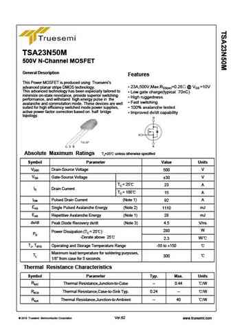
TSA23N50M 500V N-Channel MOSFET General Description Features This Power MOSFET is produced using Truesemi s advanced planar stripe DMOS technology. 23A,500V,Max.RDS(on)=0.26 @ VGS =10V This advanced technology has been especially tailored to Low gate charge(typical 70nC) minimize on-state resistance, provide superior switching High ruggedness performance, and withstand... See More ⇒
9.17. Size:809K cn minos
md23n50.pdf
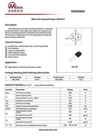
Silicon N-Channel Power MOSFET Description MD23N50 the silicon N-channel Enhanced MOSFETs, is obtained by advanced MOSFET technology which reduce the conduction loss, improve switching performance and enhance the avalanche energy. The transistor is suitable device for SMPS, high speed switching and general purpose applications. General Features 1 V =500V, R ... See More ⇒
9.18. Size:400K inchange semiconductor
irfp23n50l.pdf
iscN-Channel MOSFET Transistor IRFP23N50L FEATURES Low drain-source on-resistance RDS(ON) =0.235 (MAX) Enhancement mode Vth = 3.0 to 5.0V (VDS = 10 V, ID=0.25mA) 100% avalanche tested Minimum Lot-to-Lot variations for robust device performance and reliable operation DESCRITION Switching Voltage Regulators ABSOLUTE MAXIMUM RATINGS(T =25 ) a SYMBOL PARAMETER VA... See More ⇒
9.19. Size:301K inchange semiconductor
23n50.pdf
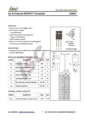
isc N-Channel MOSFET Transistor 23N50 FEATURES Drain Current I = 23A@ T =25 D C Drain Source Voltage- V =500V(Min) DSS Static Drain-Source On-Resistance R =0.245 (Max) DS(on) 100% avalanche tested Minimum Lot-to-Lot variations for robust device performance and reliable operation DESCRIPTION Designed for use in switch mode power supplies and general purpose ... See More ⇒
9.20. Size:256K inchange semiconductor
fmh23n50e.pdf
isc N-Channel MOSFET Transistor FMH23N50E FEATURES With TO-3PN packaging High speed switching Standard level gate drive Easy to use 100% avalanche tested Minimum Lot-to-Lot variations for robust device performance and reliable operation APPLICATIONS Power supply Switching applications ABSOLUTE MAXIMUM RATINGS(T =25 ) a SYMBOL PARAMETER VALUE UNIT V Drain-S... See More ⇒
Detailed specifications: DH0159E, DH0159F, DH0159I, DH019N04, DH019N04B, DH019N04D, DH019N04E, 20N65D, IRF520, 5N65C, 60N10B, 60N10D, 60N10E, 60N10F, 60N10I, AOB413, B110N04
Keywords - 23N50D MOSFET specs
23N50D cross reference
23N50D equivalent finder
23N50D pdf lookup
23N50D substitution
23N50D replacement
Can't find your MOSFET?
Learn how to find a substitute transistor by analyzing voltage, current and package compatibility