DMN6066SSD Specs and Replacement
Type Designator: DMN6066SSD
Type of Transistor: MOSFET
Type of Control Channel: N-Channel
Absolute Maximum Ratings
Pd ⓘ - Maximum Power Dissipation: 2.1 W
|Vds|ⓘ - Maximum Drain-Source Voltage: 60 V
|Vgs|ⓘ - Maximum Gate-Source Voltage: 20 V
|Id| ⓘ - Maximum Drain Current: 4.4 A
Electrical Characteristics
Cossⓘ - Output Capacitance: 502 pF
RDSonⓘ - Maximum Drain-Source On-State Resistance: 0.097 Ohm
Package: SO8
DMN6066SSD substitution
- MOSFET ⓘ Cross-Reference Search
DMN6066SSD datasheet
dmn6066ssd.pdf
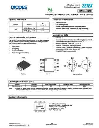
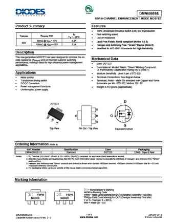
A Product Line of Diodes Incorporated DMN6066SSD 60V DUAL N-CHANNEL ENHANCEMENT MODE MOSFET Product Summary Features and Benefits Low on-resistance ID V(BR)DSS RDS(on) Fast switching speed TA = 25 C Green component and RoHS compliant (Note 1) 66m @ VGS= 10V 4.4A Qualified to AEC-Q101 Standards for High Reliability 60V 97m @ VGS= 4.5V 3.6A Me... See More ⇒
dmn6066sss.pdf
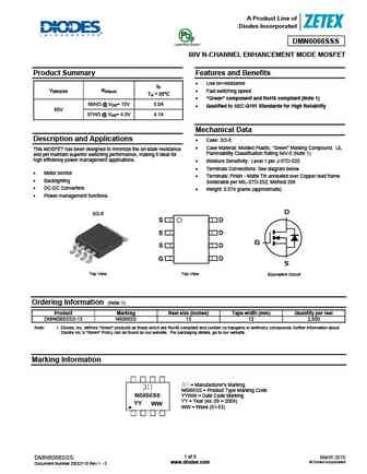
A Product Line of Diodes Incorporated DMN6066SSS 60V N-CHANNEL ENHANCEMENT MODE MOSFET Product Summary Features and Benefits Low on-resistance ID V(BR)DSS RDS(on) Fast switching speed TA = 25 C Green component and RoHS compliant (Note 1) 66m @ VGS= 10V 5.0A Qualified to AEC-Q101 Standards for High Reliability 60V 97m @ VGS= 4.5V 4.1A Mechani... See More ⇒
dmn6068lk3.pdf
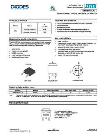
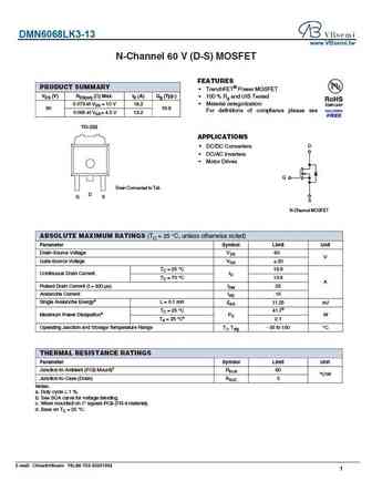
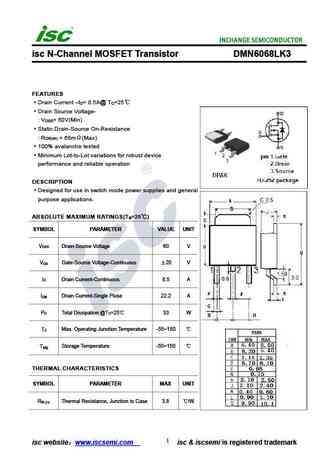
A Product Line of Diodes Incorporated DMN6068LK3 60V N-CHANNEL ENHANCEMENT MODE MOSFET Product Summary Features and Benefits 100% Unclamped Inductive Switch (UIS) test in production ID V(BR)DSS RDS(on) Low on-resistance TA = 25 C Fast switching speed 68m @ VGS= 10V 8.5A Green component and RoHS compliant (Note 1) 60V Qualified to AEC-Q101 Stan... See More ⇒
dmn6068se.pdf
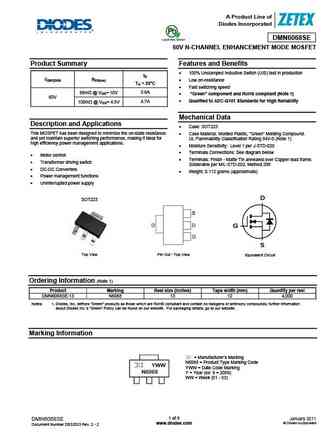
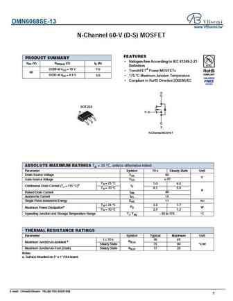
A Product Line of Diodes Incorporated DMN6068SE 60V N-CHANNEL ENHANCEMENT MODE MOSFET Product Summary Features and Benefits 100% Unclamped Inductive Switch (UIS) test in production ID V(BR)DSS RDS(on) Low on-resistance TA = 25 C Fast switching speed 68m @ VGS= 10V 5.6A Green component and RoHS compliant (Note 1) 60V Qualified to AEC-Q101 Stan... See More ⇒
Detailed specifications: DMN5L06VK, DMN5L06WK, DMN601DMK, DMN601DWK, DMN601K, DMN601TK, DMN601VK, DMN601WK, 13N50, DMN6066SSS, DMN6068LK3, DMN6068SE, DMN62D1SFB, DMN66D0LDW, DMN66D0LT, DMN66D0LW, ZXM64N035L3
Keywords - DMN6066SSD MOSFET specs
DMN6066SSD cross reference
DMN6066SSD equivalent finder
DMN6066SSD pdf lookup
DMN6066SSD substitution
DMN6066SSD replacement
Step-by-step guide to finding a MOSFET replacement. Cross-reference parts and ensure compatibility for your repair or project.
🌐 : EN ES РУ

LIST
Last Update
MOSFET: FTF30P35D | FTF25N35DHVT | FTF15N35D | FTE15C35G | FTP02P15G | FTE02P15G | AKF30N5P0SX | AKF30N10S | AKF20P45D | CM4407
Popular searches
d882 transistor equivalent | 17n80c3 | bc107 transistor | rjp63g4 datasheet | 2sc1115 | c3998 transistor | 2sa679 | 2sc3181