AGM615MNA Specs and Replacement
Type Designator: AGM615MNA
Type of Transistor: MOSFET
Type of Control Channel: N-Channel
Absolute Maximum Ratings
Pd ⓘ
- Maximum Power Dissipation: 78 W
|Vds|ⓘ - Maximum Drain-Source Voltage: 60 V
|Vgs|ⓘ - Maximum Gate-Source Voltage: 20 V
|Id| ⓘ - Maximum Drain Current: 53 A
Tj ⓘ - Maximum Junction Temperature: 150 °C
Electrical Characteristics
tr ⓘ - Rise Time: 5.1 nS
Cossⓘ -
Output Capacitance: 78 pF
RDSonⓘ - Maximum Drain-Source On-State Resistance: 0.016 Ohm
Package: PDFN5X6
- MOSFET ⓘ Cross-Reference Search
AGM615MNA datasheet
..1. Size:1137K cn agmsemi
agm615mna.pdf 
AGM615MNA Table 3. Electrical Characteristics (TJ=25 unless otherwise noted) Symbol Parameter Conditions Min Typ Max Unit On/Off States BV Drain-Source Breakdown Voltage V =0V I =250 A 60 -- -- V GS D DSS Zero Gate Voltage Drain Current V =48V,V =0V -- -- 1.0 A DS GS I DSS Gate-Body Leakage Current V = 20V,V =0V -- -- nA GS DS I GSS 100 V Gate Threshold Voltage V =V ... See More ⇒
6.1. Size:1061K cn agmsemi
agm615mn.pdf
AGM615MN Table 3. Electrical Characteristics (TJ=25 unless otherwise noted) Symbol Parameter Conditions Min Typ Max Unit On/Off States BV Drain-Source Breakdown Voltage V =0V I =250 A 60 -- -- V GS D DSS Zero Gate Voltage Drain Current V =60V,V =0V -- -- 1 A DS GS I DSS Gate-Body Leakage Current V = 20V,V =0V -- -- nA GS DS I GSS 100 V Gate Threshold Voltage V =V ,I ... See More ⇒
8.1. Size:1237K cn agmsemi
agm615d.pdf
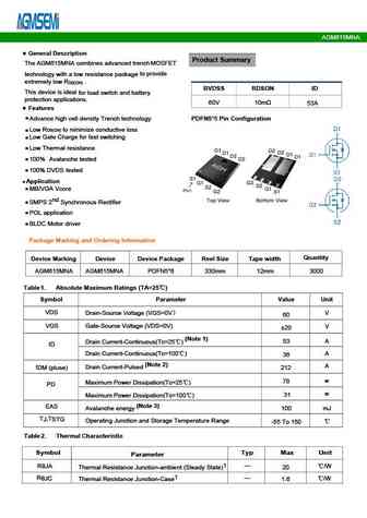
AGM615D General Description Product Summary The AGM615D combines advanced trenchMOSFET to provide technology with a low resistance package extremely low R . DS(ON) BVDSS RDSON ID This device is ideal for load switch and battery 60V 11.5m 45A protection applications. TO-252 Pin Configuration Features Advance high cell density Trench technology Low R to minimiz... See More ⇒
9.1. Size:964K cn agmsemi
agm614mn.pdf
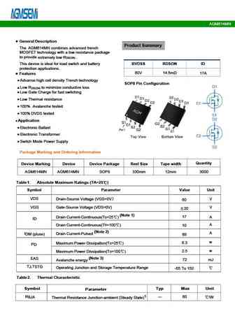
AGM614MN Table 3. Electrical Characteristics (TJ=25 unless otherwise noted) Symbol Parameter Conditions Min Typ Max Unit On/Off States BVDSS Drain-Source Breakdown Voltage V =0V I =250 A GS D 60 -- -- V Zero Gate Voltage Drain Current V =60V,V =0V -- -- 1 A DS GS I DSS Gate-Body Leakage Current V = 20V,V =0V -- -- GS DS nA I GSS 100 VGS(th) Gate Threshold Voltage V ... See More ⇒
9.2. Size:980K cn agmsemi
agm612mbq.pdf
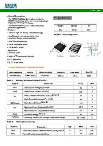
AGM612MBQ Table 3. Electrical Characteristics (TJ=25 unless otherwise noted) Symbol Parameter Conditions Min Typ Max Unit On/Off States BV Drain-Source Breakdown Voltage V =0V I =250 A 60 -- -- V GS D DSS Zero Gate Voltage Drain Current V =60V,V =0V -- -- 1 A DS GS I DSS Gate-Body Leakage Current V = 20V,V =0V -- -- nA GS DS I GSS 100 V Gate Threshold Voltage V =V ,I... See More ⇒
9.3. Size:997K cn agmsemi
agm614mbp.pdf
AGM614MBP Typical Characteristics Fig.1 Typical Output Characteristics Fig.2 On-Resistance vs G-S Voltage Fig.3 Source Drain Forward Characteristics Fig.4 Gate-Charge Characteristics Fig.5 Normalized V vs T Fig.6 Normalized R vs T GS(th) J DSON J www.agm-mos.com 3 VER2.66 AGM614MBP Fig.7 Capacitance Fig.8 Safe Operating Area 1 DUTY=0.5 0.2 0.1 0.1 0.05 PDM TON 0.02 T 0... See More ⇒
9.4. Size:1421K cn agmsemi
agm612d.pdf
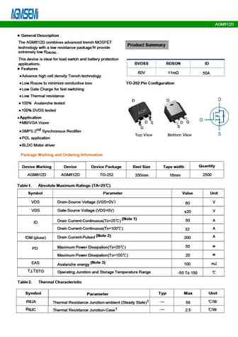
AGM612D Table 3. Electrical Characteristics (TJ=25 unless otherwise noted) Symbol Parameter Conditions Min Typ Max Unit On/Off States BV Drain-Source Breakdown Voltage V =0V I =250 A 60 -- -- V GS D DSS Zero Gate Voltage Drain Current V =60V,V =0V -- -- 1.0 A DS GS I DSS Gate-Body Leakage Current V = 20V,V =0V -- -- nA GS DS I GSS 100 V Gate Threshold Voltage V =V ,I... See More ⇒
9.5. Size:1190K cn agmsemi
agm612mn.pdf
AGM612MN Typical Characteristics Power Capability Current Capability 1.2 18 16 1.0 14 0.9 12 0.8 10 0.7 8 0.6 6 0.5 4 0.4 2 TC=25oC,VG=10V TC=25oC 0.3 0 0 20 40 60 80 100 120 140 160 180 0 20 40 60 80 100 120 140 160 Tmp Mounting Point Temp. ( Tmp Mounting Point Temp. ( C) C) Safe Operating Area Transient Thermal Impedance 200 2 100 1 Duty = 0.5 ... See More ⇒
9.6. Size:839K cn agmsemi
agm614d.pdf
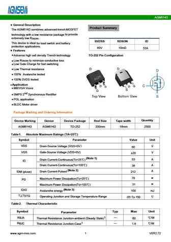
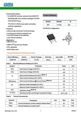
AGM614D General Description Product Summary The AGM614D combines advanced trenchMOSFET to provide technology with a low resistance package extremely low R . DS(ON) BVDSS RDSON ID This device is ideal for load switch and battery protection applications. 60V 10m 53A Features Advance high cell density Trench technology TO-252 Pin Configuration Low R to minimize c... See More ⇒
9.7. Size:1226K cn agmsemi
agm614mna.pdf
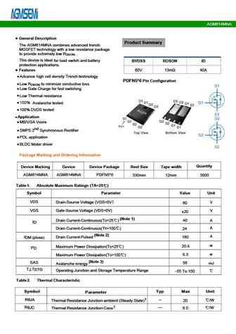
AGM614MNA Table 3. Electrical Characteristics (TJ=25 unless otherwise noted) Symbol Parameter Conditions Min Typ Max Unit On/Off States BV Drain-Source Breakdown Voltage V =0V I =250 A 60 -- -- V GS D DSS Zero Gate Voltage Drain Current V =60V,V =0V -- -- 1 A DS GS I DSS Gate-Body Leakage Current V = 20V,V =0V -- -- nA GS DS I GSS 100 V Gate Threshold Voltage V =V ,I... See More ⇒
9.8. Size:1243K cn agmsemi
agm612ap.pdf
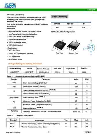
AGM612AP General Description Product Summary The AGM612AP combines advanced trench MOSFET to technology with a low resistance package provide extremely low R . DS(ON) BVDSS RDSON ID This device is ideal load switch and battery protection for applications. 60V 11m 50A Features Advance high cell density Trench technology PDFN3.3*3.3 Pin Configuration Low R to m... See More ⇒
9.9. Size:1330K cn agmsemi
agm612mna.pdf
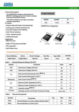
AGM612MNA Table 3. Electrical Characteristics (TJ=25 unless otherwise noted) Symbol Parameter Conditions Min Typ Max Unit On/Off States BVDSS Drain-Source Breakdown Voltage V =0V I =250 A 60 -- -- V GS D Zero Gate Voltage Drain Current V =60V,V =0V -- -- 1 A DS GS I DSS Gate-Body Leakage Current V = 20V,V =0V -- -- nA GS DS I GSS 100 V Gate Threshold Voltage V =V ,I =... See More ⇒
9.10. Size:979K cn agmsemi
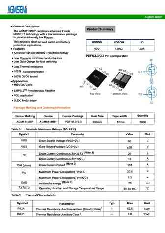
agm612mbp.pdf
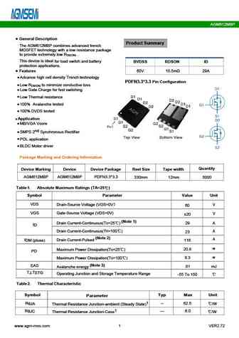
AGM612MBP General Description Product Summary The AGM612MBP combines advanced trench MOSFET technology with a low resistance package to provide extremely low R . DS(ON) This device is ideal for load switch and battery BVDSS RDSON ID protection applications. Features 60V 10.5m 29A Advance high cell density Trench technology PDFN3.3*3.3 Pin Configuration Low R to ... See More ⇒
9.11. Size:1515K cn agmsemi
agm614a-g.pdf
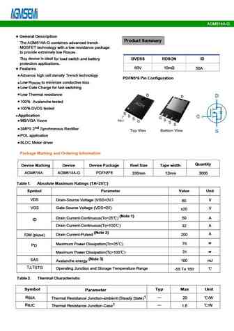
AGM614A-G Table 3. Electrical Characteristics (TJ=25 unless otherwise noted) Symbol Parameter Conditions Min Typ Max Unit On/Off States BV Drain-Source Breakdown Voltage V =0V I =250 A 60 -- -- V GS D DSS Zero Gate Voltage Drain Current V =60V,V =0V -- -- 1.0 A DS GS I DSS Gate-Body Leakage Current V = 20V,V =0V -- -- nA GS DS I GSS 100 V Gate Threshold Voltage V =V ... See More ⇒
9.12. Size:969K cn agmsemi
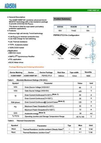
agm614mbp-m1.pdf
AGM614MBP-M1 Electrical characteristics diagrams Fig.1 Typ. transfer characteristics Fig.2 Typ. output characteristics 80 80 VDS=5V 10V 8V 7V 60 60 6V 40 40 5.5V 20 150 20 5V 25 -55 VGS=4.5V 0 0 0 2 4 6 8 10 0 1 2 3 4 5 V (V) V (V) GS DS Fig.3 Normalized on-resistance vs drain current Fig.4 Typ. on-resistance vs gate-source voltage 50 5 ID=30A 40 4... See More ⇒
9.13. Size:1036K cn agmsemi
agm610m.pdf
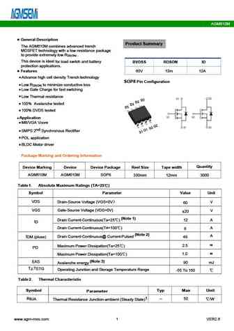
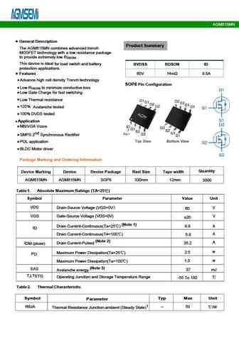
AGM610M General Description Product Summary The AGM610M combines advanced trench MOSFET technology with a low resistance package to provide extremely low R . DS(ON) This device is ideal for load switch and battery BVDSS RDSON ID protection applications. Features 60V 12m 12A Advance high cell density Trench technology SOP8 Pin Configuration Low R to minimize conduc... See More ⇒
9.14. Size:1109K cn agmsemi
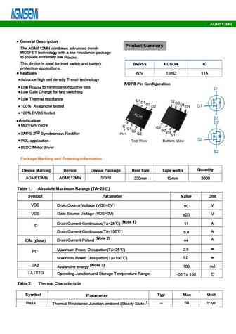
agm612s.pdf
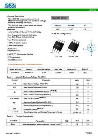
AGM612S General Description Product Summary The AGM612S combines advanced trench MOSFET technology with a low resistance package to provide extremely low R . DS(ON) This device is ideal for load switch and battery BVDSS RDSON ID protection applications. Features 60V 11m 11A Advance high cell density Trench technology SOP8 Pin Configuration Low R to minimize cond... See More ⇒
9.15. Size:1357K cn agmsemi
agm610mn.pdf
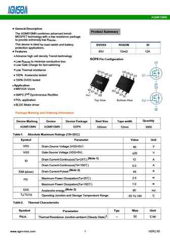
AGM610MN General Description Product Summary The AGM610MN combines advanced trench MOSFET technology with a low resistance package to provide extremely low R . DS(ON) This device is ideal for load switch and battery BVDSS RDSON ID protection applications. Features 60V 12m 12A Advance high cell density Trench technology SOP8 Pin Configuration Low R to minimize co... See More ⇒
Detailed specifications: AGM614A-G, AGM614D, AGM614MBP, AGM614MBP-M1, AGM614MN, AGM614MNA, AGM615D, AGM615MN, STP75NF75, FTP16N06A, HCA60R070F, HYG043N10NS2P, HYG043N10NS2B, RM150N100HD, SLB40N26C, SLI40N26C, AGM404D
Keywords - AGM615MNA MOSFET specs
AGM615MNA cross reference
AGM615MNA equivalent finder
AGM615MNA pdf lookup
AGM615MNA substitution
AGM615MNA replacement
Step-by-step guide to finding a MOSFET replacement. Cross-reference parts and ensure compatibility for your repair or project.
