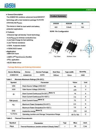
AGM408M Specs and Replacement
Type Designator: AGM408M
Type of Transistor: MOSFET
Type of Control Channel: N-Channel
Absolute Maximum Ratings
Pd ⓘ - Maximum Power Dissipation: 2.5 W
|Vds|ⓘ - Maximum Drain-Source Voltage: 40 V
|Vgs|ⓘ - Maximum Gate-Source Voltage: 20 V
|Id| ⓘ - Maximum Drain Current: 7.5 A
Tj ⓘ - Maximum Junction Temperature: 150 °C
Electrical Characteristics
tr ⓘ - Rise Time: 3.4 nS
Cossⓘ - Output Capacitance: 120 pF
RDSonⓘ - Maximum Drain-Source On-State Resistance: 0.015 Ohm
Package: SOP8
AGM408M substitution
- MOSFET ⓘ Cross-Reference Search
AGM408M datasheet
agm408m.pdf
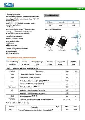
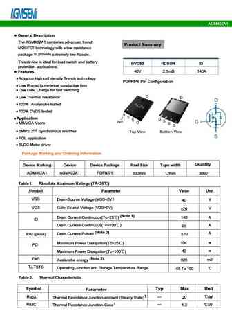
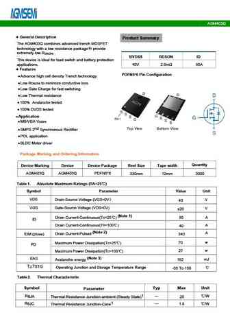
AGM408M Table 3. Electrical Characteristics (TJ=25 unless otherwise noted) Symbol Parameter Conditions Min Typ Max Unit On/Off States BV Drain-Source Breakdown Voltage V =0V I =250 A 40 -- -- V GS D DSS Zero Gate Voltage Drain Current V =40V,V =0V -- -- 1 A DS GS I DSS Gate-Body Leakage Current V = 20V,V =0V -- -- nA GS DS I GSS 100 V Gate Threshold Voltage V =V ,I =... See More ⇒
agm408mn.pdf
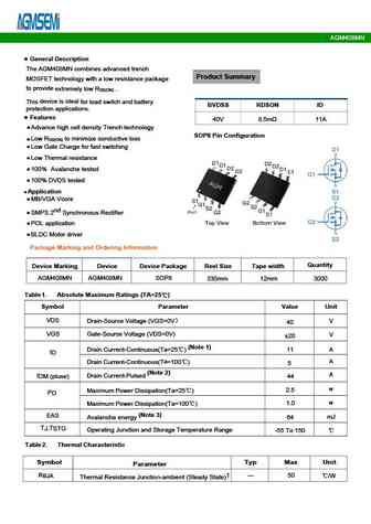
AGM408MN Typical Characteristics 2.7 40 10V,6V,5V,4.5V,4V IDS= 250uA 2.4 Max 2.1 30 VGS= 3.5V 1.8 Typ 1.5 20 1.2 Min 0.9 10 VGS= 3V Notes 0.6 1. 250 s pulse test 2. Tj=25 C 0.3 0 0 25 50 75 100 125 150 175 0 1 2 3 4 5 VDS, Drain -Source Voltage (V) Tj - Junction Temperature ( C) Fig1. Typical Output Characteristics Fig2. Typical V Gate -Source Voltage Vs. T... See More ⇒
agm40p25a.pdf
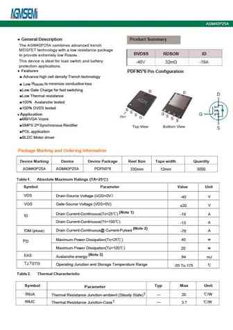
AGM40P25A Table 2. P-Channel Electrical Characteristics (TJ=25 unless otherwisenoted) Symbol Parameter Conditions Min Typ Max Unit On/Off States BVDSS Drain-Source Breakdown Voltage VGS=0V ID=-250 A -40 -- -- V Zero Gate Voltage Drain Current V =-40V,V =0V -1 DS GS I -- -- A DSS Gate-Body Leakage Current V = 20V,V =0V 100 GS DS I -- -- nA GSS V Gate Threshold Voltage V =V... See More ⇒
agm402c.pdf
AGM402C Typical Characteristics VDS, Drain -Source Voltage (V) Tj - Junction Temperature ( C) Fig1. Typical Output Characteristics Fig2. VGS(TH) Gate -Source Voltage Vs. Tj VGS, Gate -Source Voltage (V) Tj - Junction Temperature ( C) Fig3. Typical Transfer Characteristics Fig4. Normalized On-Resistance Vs. Temperature VSD, Source-Drain Voltage (V) VDS, Drain -Source Voltage (V)... See More ⇒
agm405ap1.pdf

AGM405AP1 Table 3. Electrical Characteristics (TJ=25 unless otherwise noted) Symbol Parameter Conditions Min Typ Max Unit On/Off States BV Drain-Source Breakdown Voltage V =0V I =250 A 40 -- -- V GS D DSS Zero Gate Voltage Drain Current V =40V,V =0V -- -- 1 A DS GS I DSS Gate-Body Leakage Current V = 20V,V =0V -- -- nA GS DS I GSS 100 V Gate Threshold Voltage V =V ,I... See More ⇒
agm401ll.pdf
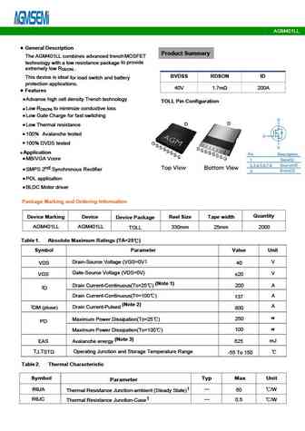
AGM401LL Table 3. Electrical Characteristics (TJ=25 unless otherwise noted) Symbol Parameter Conditions Min Typ Max Unit On/Off States BV Drain-Source Breakdown Voltage V =0V I =250 A 40 45 -- V GS D DSS Zero Gate Voltage Drain Current V =40V,V =0V -- -- 1 A DS GS I DSS Gate-Body Leakage Current V = 20V,V =0V -- -- nA GS DS I GSS 100 -- V Gate Threshold Voltage V =V... See More ⇒
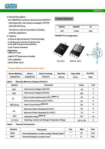
agm40p30d.pdf
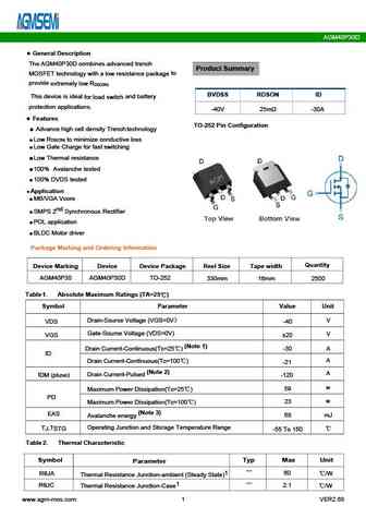
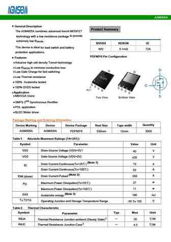
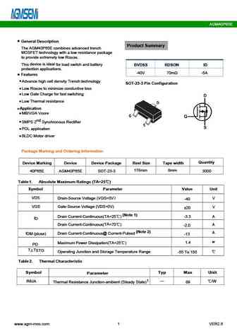
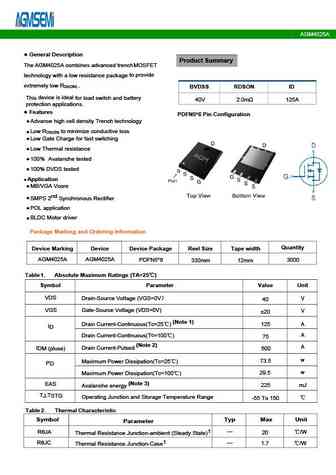
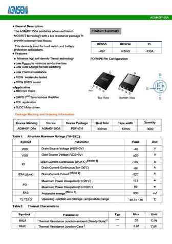
AGM40P30D General Description The AGM40P30D combines advanced trench Product Summary to MOSFET technology with a low resistance package provide extremely low R DS(ON) BVDSS RDSON ID This device is ideal and battery for load switch protection applications. -40V 25m -30A Features TO-252 Pin Configuration Advance high cell density Trench technology Low R to minimize ... See More ⇒
agm404a.pdf
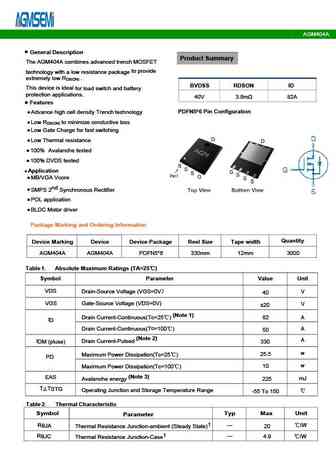
AGM404A Typical Performance Characteristics Figure 2 Typical Transfer Characteristics Figure1 Output Characteristics ID (A) ID (A) 120 120 10V 100 100 4.5V 4V 80 80 60 60 3.5V 40 40 125 25 20 20 VGS=3V VDS(V) VGS(V) 0 0 0 1.0 2.0 3.0 4.0 5.0 0 2 4 6 8 10 Figure 4 Body Diode Characteristics Figure 3 On-resistance vs. Drain Current IS(A) RDS(ON) (m ) ... See More ⇒
agm409a.pdf
AGM409A Typical Characteristics VDS, Drain -Source Voltage (V) Tj - Junction Temperature ( C) Fig1. Typical Output Characteristics Fig2. VGS(TH) Gate -Source Voltage Vs.Tj VGS, Gate -Source Voltage (V) Tj - Junction Temperature ( C) Fig3. Typical Transfer Characteristics Fig4. Normalized On-Resistance Vs. Tj VSD, Source-Drain Voltage (V) VDS, Drain -Source Voltage (V) Fig5. T... See More ⇒
agm40p35a.pdf
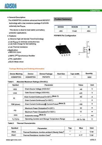
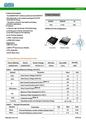
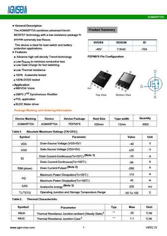
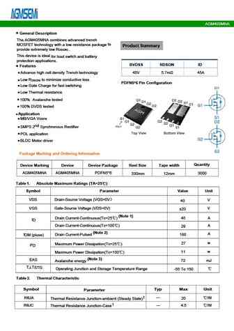
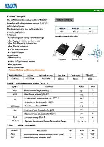
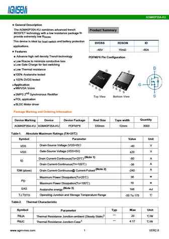
AGM40P35A General Description Product Summary The AGM40P35A combines advanced trench MOSFET to provide technology with a low resistance package extremely low R DS(ON) BVDSS RDSON ID This device is ideal and battery for load switch -40V 11m -60A protection applications. PDFN5*6 Pin Configuration Features Advance high cell density Trench technology Low R to minimize ... See More ⇒
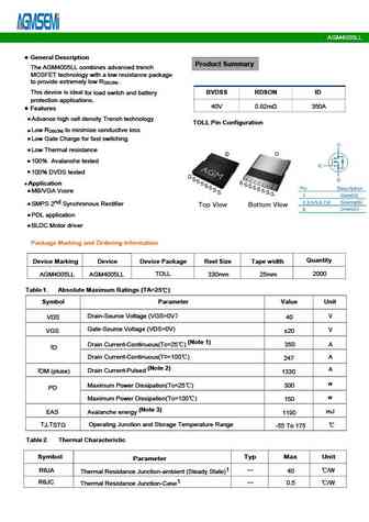
agm4005llm1.pdf
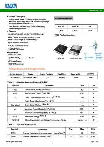
AGM4005LLM1 General Description Product Summary The AGM4005LLM1 combines advanced trench MOSFET technology with a low resistance package to provide extremely low R . DS(ON) This device is ideal BVDSS RDSON ID for load switch and battery protection applications. 40V 0.92m 330A Features Advance high cell density Trench technology TOLL Pin Configuration Low R to mi... See More ⇒
agm403a1.pdf
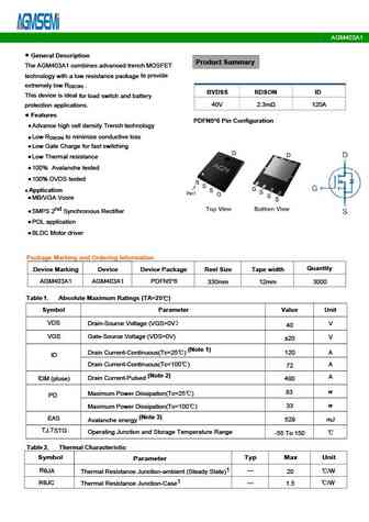
AGM403A1 Table 3. Electrical Characteristics (TJ=25 unless otherwise noted) Symbol Parameter Conditions Min Typ Max Unit On/Off States BV Drain-Source Breakdown Voltage V =0V I =250 A 40 -- -- V GS D DSS Zero Gate Voltage Drain Current V =40V,V =0V -- -- 1 A DS GS I DSS V = 20V,V =0V -- -- nA GS DS IGSS Gate-Body Leakage Current 100 VGS(th) Gate Threshold Voltage V ... See More ⇒
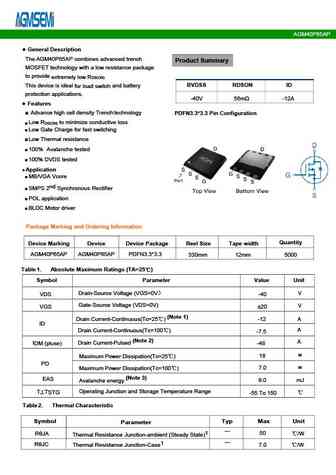
agm40p55ap.pdf
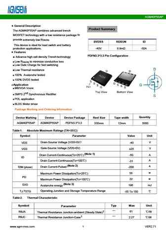
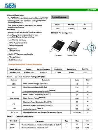
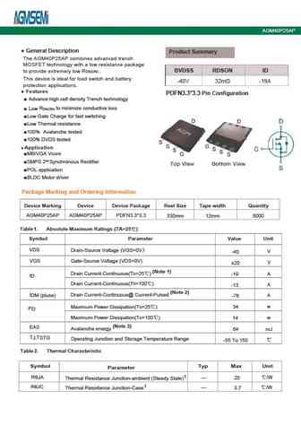
AGM40P55AP General Description Product Summary The AGM40P55AP combines advanced trench to MOSFET technology with a low resistance package provide extremely low R DS(ON) BVDSS RDSON ID This device is ideal for load switch and battery protection applications. -40V 8.9m -50A Features PDFN3.3*3.3 Pin Configuration Advance high cell density Trench technology Low R to min... See More ⇒
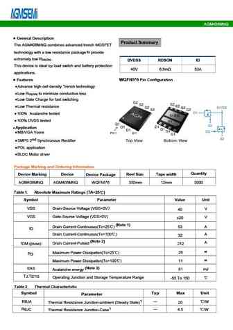
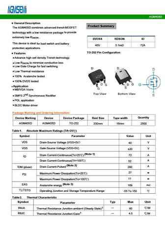
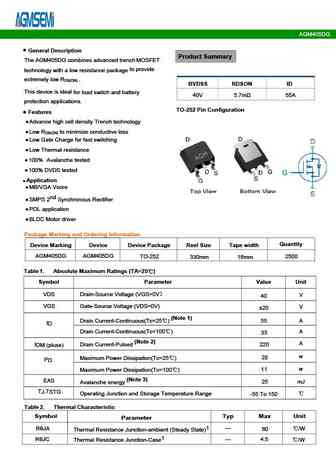
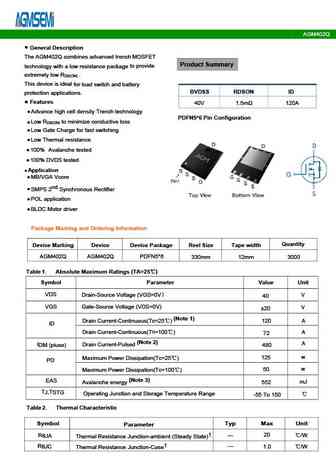
agm406mbq.pdf
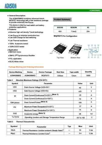
AGM406MBQ Table 3. Electrical Characteristics (TJ=25 unless otherwise noted) Symbol Parameter Conditions Min Typ Max Unit On/Off States BV Drain-Source Breakdown Voltage V =0V I =250 A 40 -- -- V GS D DSS Zero Gate Voltage Drain Current V =40V,V =0V -- -- 1 A DS GS I DSS Gate-Body Leakage Current V = 20V,V =0V -- -- nA GS DS I 100 GSS V Gate Threshold Voltage V =V ,I =2... See More ⇒
agm401c.pdf
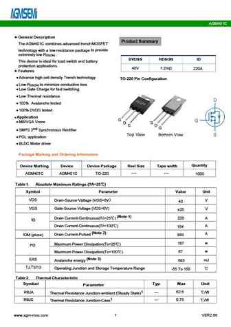
AGM401C General Description Product Summary The AGM401C combines advanced trenchMOSFET to provide technology with a low resistance package extremely low R . DS(ON) BVDSS RDSON ID This device is ideal for load switch and battery protection applications. 40V 1.2m 220A Features Advance high cell density Trench technology TO-220 Pin Configuration Low R to minimize... See More ⇒
agm402c1.pdf
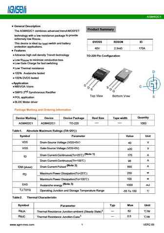
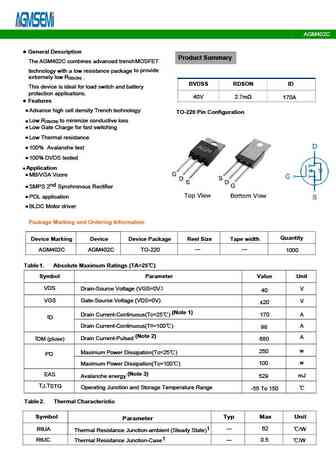
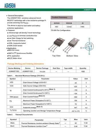
AGM402C1 General Description Product Summary The AGM402C1 combines advanced trenchMOSFET to provide technology with a low resistance package extremely low R . DS(ON) BVDSS RDSON ID This device is ideal for load switch and battery protection applications. 40V 2.3m 170A Features Advance high cell density Trench technology TO-220 Pin Configuration Low R to minimiz... See More ⇒
agm40p100h.pdf
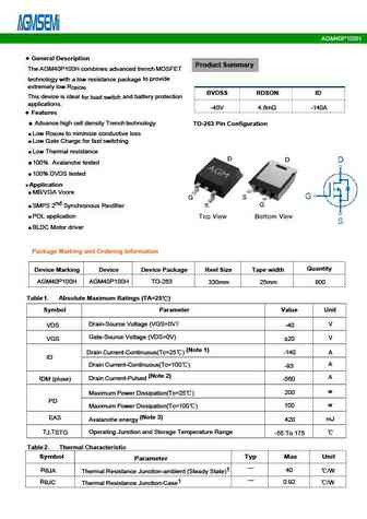
AGM40P100H Table 3. Electrical Characteristics (TJ=25 unless otherwise noted) Symbol Parameter Conditions Min Typ Max Unit On/Off States BVDSS Drain-Source Breakdown Voltage V =0V I =-250 A -40 -- -- V GS D Zero Gate Voltage Drain Current V =-40V,V =0V -- -- -1 A DS GS I DSS Gate-Body Leakage Current V = 20V,V =0V -- -- 100 nA GS DS I GSS VGS(th) Gate Threshold Voltage... See More ⇒
agm402a1.pdf
AGM402A1 Typical Characteristics VDS, Drain -Source Voltage (V) Tj - Junction Temperature ( C) Fig1. Typical Output Characteristics Fig2. VGS(TH) Gate -Source Voltage Vs. Tj VGS, Gate -Source Voltage (V) Tj - Junction Temperature ( C) Fig3. Typical Transfer Characteristics Fig4. Normalized On-Resistance Vs. Temperature VSD, Source-Drain Voltage (V) VDS, Drain -Source Voltage (V... See More ⇒
agm403q.pdf
AGM403Q N-Channel Typical Characteristics Fig.1 Typical Output Characteristics Fig.2 On-Resistance vs G-S Voltage Fig.3 Source Drain Forward Characteristics Fig.4 Gate-Charge Characteristics 1.8 1.8 1.4 1.4 1.0 1 0.6 0.6 0.2 0.2 -50 0 50 100 150 -50 0 50 100 150 TJ ,Junction Temperature ( ) TJ , Junction Temperature ( ) Fig.5 Normalized V vs T Fig.6 Normalized R vs T ... See More ⇒
agm40p26e.pdf
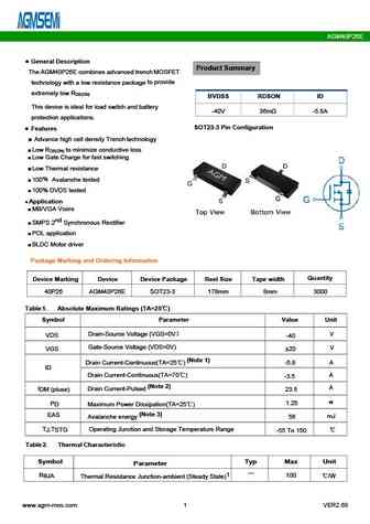
AGM40P26E General Description Product Summary The AGM40P26E combines advanced trench MOSFET to provide technology with a low resistance package extremely low R DS(ON) BVDSS RDSON ID This device is ideal and battery for load switch -40V 36m -5.8A protection applications. SOT23-3 Pin Configuration Features Advance high cell density Trench technology Low R to minimize... See More ⇒
agm40p55d.pdf
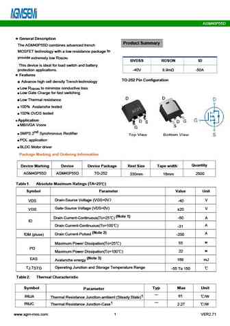
AGM40P55D General Description Product Summary The AGM40P55D combines advanced trench to MOSFET technology with a low resistance package provide extremely low R DS(ON) BVDSS RDSON ID This device is ideal for load switch and battery protection applications. -40V 8.9m -50A Features TO-252 Pin Configuration Advance high cell density Trench technology Low R to minimize c... See More ⇒
agm405a.pdf
AGM405A Typical Performance Characteristics Figure 2 Typical Transfer Characteristics Figure1 Output Characteristics ID (A) ID (A) 150 100 5V 10V VDS=5V 4V 120 80 6V 3.5V 25 60 90 60 40 125 VGS=3V 30 20 VGS(V) VDS(V) 0 0 0 0.5 1.0 1.5 2.0 2.5 3.0 3.5 4.0 4.5 5.0 2 2.5 3 3.5 4 4.5 Figure 4 Body Diode Characteristics Figure 3 On-resistance vs. Drain Current I... See More ⇒
agm40p13s.pdf
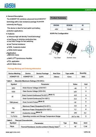
AGM40P13S General Description Product Summary The AGM40P13S combines advanced trench MOSFET to provide technology with a low resistance package extremely low R DS(ON) BVDSS RDSON ID This device is ideal and battery for load switch -40V 13m -8A protection applications. SOP8 Pin Configuration Features Advance high cell density Trench technology Low R to minimize cond... See More ⇒
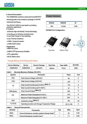
agm4025d.pdf
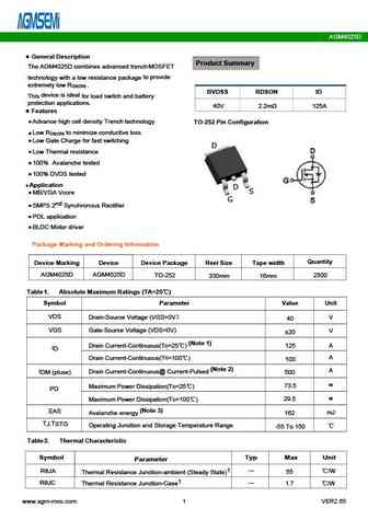
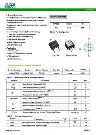
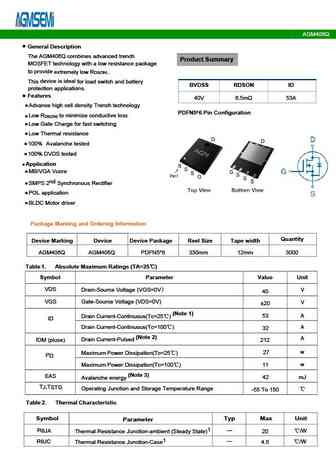
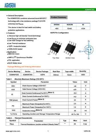
AGM4025D General Description Product Summary The AGM4025D combines advanced trenchMOSFET to provide technology with a low resistance package extremely low R . DS(ON) BVDSS RDSON ID device is ideal This for load switch and battery protection applications. 40V 2.2m 125A Features Advance high cell density Trench technology TO-252 Pin Configuration Low R to minimi... See More ⇒
agm4025q.pdf
AGM4025Q N-Channel Typical Characteristics Fig.1 Typical Output Characteristics Fig.2 On-Resistance vs G-S Voltage Fig.3 Source Drain Forward Characteristics Fig.4 Gate-Charge Characteristics 1.8 1.8 1.4 1.4 1.0 1 0.6 0.6 0.2 0.2 -50 0 50 100 150 -50 0 50 100 150 TJ ,Junction Temperature ( ) TJ , Junction Temperature ( ) Fig.5 Normalized V vs T Fig.6 Normalized R vs T ... See More ⇒
agm404q.pdf
AGM404Q Electrical Characteristics Diagrams 100 50 VGS = 6 V VDS = 5 V 90 VGS = 4.5 V 80 40 VGS = 4 V 70 VGS = 10 V 60 30 VGS = 3.5 V 50 40 20 30 125 25 VGS = 3 V 20 10 10 0 0 0 0.5 1 1.5 2 0 1 2 3 4 5 6 VGS (V) VDS (V) Figure 2 Transfer Characteristics Figure 1 On-Region Characteristics 10 2.1 9 1.9 VGS = 4.5 V VGS = 10 V 8 1.7 ID = 20 A 7 1.5 6 1... See More ⇒
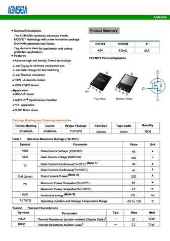
agm4012a.pdf
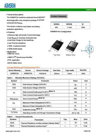
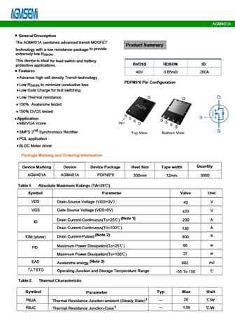
AGM4012A General Description Product Summary The AGM4012A combines advanced trench MOSFET to provide technology with a low resistance package extremely low R . DS(ON) BVDSS RDSON ID This device is ideal for load switch and battery 40V 1.1m 160A protection applications. PDFN5*6 Pin Configuration Features Advance high cell density Trench technology Low R to mini... See More ⇒
agm405mbp.pdf

AGM405MBP Table 3. Electrical Characteristics (TJ=25 unless otherwise noted) Symbol Parameter Conditions Min Typ Max Unit On/Off States BVDSS Drain-Source Breakdown Voltage V =0V I =250 A GS D 40 -- -- V Zero Gate Voltage Drain Current V =40V,V =0V -- -- 1 A DS GS I DSS Gate-Body Leakage Current V = 20V,V =0V -- -- nA GS DS I GSS 100 VGS(th) Gate Threshold Voltage V... See More ⇒
agm406mnq.pdf
AGM406MNQ Table 3. Electrical Characteristics (TJ=25 unless otherwise noted) Symbol Parameter Conditions Min Typ Max Unit On/Off States BV Drain-Source Breakdown Voltage V =0V I =250 A 40 -- -- V GS D DSS Zero Gate Voltage Drain Current V =40V,V =0V -- -- 1 A DS GS I DSS Gate-Body Leakage Current V = 20V,V =0V -- -- nA GS DS I GSS 100 V Gate Threshold Voltage V =V ,I... See More ⇒
agm40p65ap.pdf
AGM40P65AP Typical Characteristics -VDS, - Drain -Source Voltage (V) Tj - Junction Temperature ( C) Fig1. Typical Output Characteristics Fig2. -V Gate -Source Voltage Vs. Tj GS(TH) -VGS, -Gate -Source Voltage (V) Tj - Junction Temperature ( C) Fig3. Typical Transfer Characteristics Fig4. Normalized On-Resistance Vs. Tj -VSD, -Source-Drain Voltage (V) -VDS, -Drain -Source Voltage (V) ... See More ⇒
agm402h.pdf
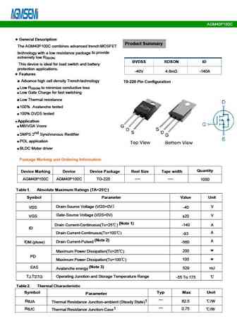
AGM402H General Description Product Summary The AGM402H combines advanced trench MOSFET to provide technology with a low resistance package extremely low R . DS(ON) BVDSS RDSON ID This device is ideal for load switch and battery 40V 2.6m 170A protection applications. Features TO-263 Pin Configuration Advance high cell density Trench technology Low R to minimize ... See More ⇒
agm405d.pdf
AGM405D Typical Performance Characteristics Figure 2 Typical Transfer Characteristics Figure1 Output Characteristics ID (A) ID (A) 150 100 5V 10V VDS=5V 4V 120 80 6V 3.5V 25 60 90 60 40 125 VGS=3V 30 20 VGS(V) VDS(V) 0 0 0 0.5 1.0 1.5 2.0 2.5 3.0 3.5 4.0 4.5 5.0 2 2.5 3 3.5 4 4.5 Figure 4 Body Diode Characteristics Figure 3 On-resistance vs. Drain Current I... See More ⇒
agm40p30ap.pdf
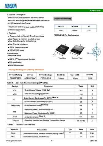
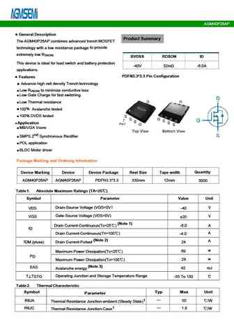
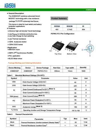
AGM40P30AP General Description The AGM40P30AP combines advanced trench Product Summary to MOSFET technology with a low resistance package provide extremely low R DS(ON) BVDSS RDSON ID This device is ideal and battery for load switch protection applications. -40V 26m -33A Features PDFN3.3*3.3 Pin Configuration Advance high cell density Trench technology Low R to mi... See More ⇒
agm405dg.pdf
AGM405DG Table 3. Electrical Characteristics (TJ=25 unless otherwise noted) Symbol Parameter Conditions Min Typ Max Unit On/Off States BV Drain-Source Breakdown Voltage V =0V I =250 A 40 -- -- V GS D DSS Zero Gate Voltage Drain Current V =40V,V =0V -- -- 1 A DS GS I DSS V = 20V,V =0V -- -- nA GS DS IGSS Gate-Body Leakage Current 100 VGS(th) Gate Threshold Voltage V ... See More ⇒
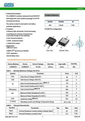
agm402d.pdf
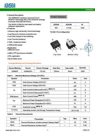
AGM402D General Description Product Summary The AGM402D combines advanced trenchMOSFET to provide technology with a low resistance package extremely low R . DS(ON) BVDSS RDSON ID This device is ideal for load switch and battery 40V 2.4m 125A protection applications. TO-252 Pin Configuration Features Advance high cell density Trench technology Low R to minimize... See More ⇒
agm403d1.pdf
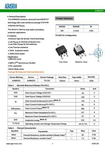
AGM403D1 General Description Product Summary The AGM403D1 combines advanced trench MOSFET technology with a low resistance package to provide extremely low R . DS(ON) device is ideal This for load switch and battery BVDSS RDSON ID protection applications. 40V 2.7m 120A Features Advance high cell density Trench technology TO-252 Pin Configuration Low R to minim... See More ⇒
agm40p26ap.pdf
AGM40P26AP Table 3. Electrical Characteristics (TJ=25 unless otherwise noted) Symbol Parameter Conditions Min Typ Max Unit On/Off States BVDSS Drain-Source Breakdown Voltage V =0V I =-250 A -40 -- -- V GS D Zero Gate Voltage Drain Current V =-40V,V =0V -- -- -1 A DS GS I DSS Gate-Body Leakage Current V = 20V,V =0V -- -- 100 nA GS DS I GSS VGS(th) Gate Threshold Voltage... See More ⇒
agm406ap.pdf
AGM406AP Table 3. Electrical Characteristics (TJ=25 unless otherwise noted) Symbol Parameter Conditions Min Typ Max Unit On/Off States BV Drain-Source Breakdown Voltage V =0V I =250 A 40 -- -- V GS D DSS Zero Gate Voltage Drain Current V =40V,V =0V -- -- 1 A DS GS I DSS Gate-Body Leakage Current V = 20V,V =0V -- -- nA GS DS I GSS 100 V Gate Threshold Voltage V =V ,I ... See More ⇒
agm40p65e.pdf
AGM40P65E General Description Product Summary The AGM40P65E combines advanced trench MOSFET technology with a low resistance package to provide extremely low R . DS(ON) device is ideal This for load switch and battery BVDSS RDSON ID protection applications. -40V 70m -5A Features Advance high cell density Trench technology SOT-23-3 Pin Configuration Low R to mi... See More ⇒
agm405f.pdf

AGM405F Typical Performance Characteristics Figure 2 Typical Transfer Characteristics Figure1 Output Characteristics ID (A) ID (A) 150 100 5V 10V VDS=5V 4V 120 80 6V 3.5V 25 60 90 60 40 125 VGS=3V 30 20 VGS(V) VDS(V) 0 0 0 0.5 1.0 1.5 2.0 2.5 3.0 3.5 4.0 4.5 5.0 2 2.5 3 3.5 4 4.5 Figure 4 Body Diode Characteristics Figure 3 On-resistance vs. Drain Current I... See More ⇒
agm40p75d.pdf
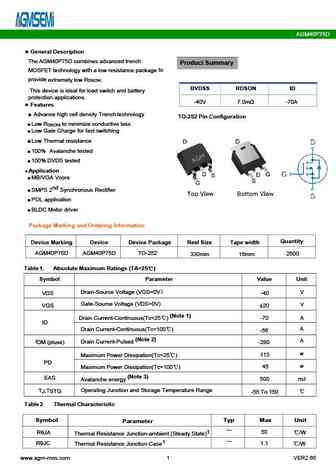
AGM40P75D General Description The AGM40P75D combines advanced trench Product Summary to MOSFET technology with a low resistance package provide extremely low R DS(ON) BVDSS RDSON ID This device is ideal for load switch and battery protection applications. -40V 7.0m -70A Features Advance high cell density Trench technology TO-252 Pin Configuration Low R to minimize ... See More ⇒
agm409d.pdf
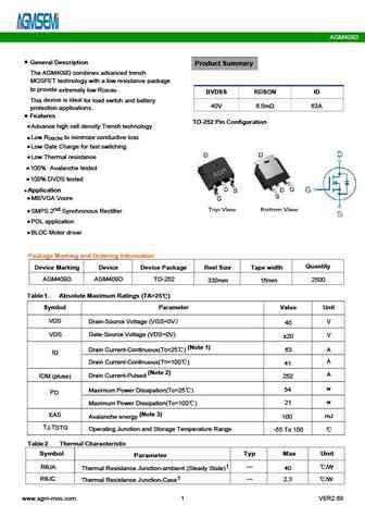
AGM409D General Description Product Summary The AGM409D combines advanced trench MOSFET technology with a low resistance package to provide extremely low R . DS(ON) BVDSS RDSON ID device is ideal This for load switch and battery 40V 6.5m 63A protection applications. Features TO-252 Pin Configuration Advance high cell density Trench technology Low R to minimize... See More ⇒
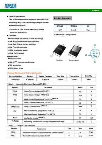
agm404ap1.pdf
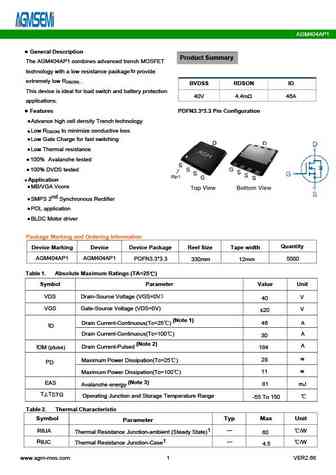
AGM404AP1 General Description Product Summary The AGM404AP1 combines advanced trench MOSFET to technology with a low resistance package provide extremely low R . DS(ON) BVDSS RDSON ID This device is ideal load switch and battery protection for 40V 4.4m 46A applications. Features PDFN3.3*3.3 Pin Configuration Advance high cell density Trench technology Low R to... See More ⇒
agm4005ll.pdf
AGM4005LL Table 3. Electrical Characteristics (TJ=25 unless otherwise noted) Symbol Parameter Conditions Min Typ Max Unit On/Off States BV Drain-Source Breakdown Voltage V =0V I =250 A 40 45 -- V GS D DSS Zero Gate Voltage Drain Current V =40V,V =0V -- -- 1 A DS GS I DSS Gate-Body Leakage Current V = 20V,V =0V -- -- nA GS DS I GSS 100 V Gate Threshold Voltage V =V ,I... See More ⇒
agm4018s.pdf
AGM4018S Table 3. Electrical Characteristics (TJ=25 unless otherwise noted) Symbol Parameter Conditions Min Typ Max Unit On/Off States BVDSS Drain-Source Breakdown Voltage V =0V I =250 A 48 -- -- V GS D Zero Gate Voltage Drain Current V =40V,V =0V -- -- 1 A DS GS I DSS Gate-Body Leakage Current V = 20V,V =0V -- -- nA GS DS I GSS 100 V Gate Threshold Voltage V =V ,I =-... See More ⇒
agm40p35ap.pdf
AGM40P35AP General Description Product Summary The AGM40P35AP combines advanced trench MOSFET to provide technology with a low resistance package extremely low R DS(ON) BVDSS RDSON ID This device is ideal for load switch and battery protection applications. -40V 11m -35A Features Advance high cell density Trench technology PDFN3.3*3.3 Pin Configuration Low R to mini... See More ⇒
agm404d.pdf
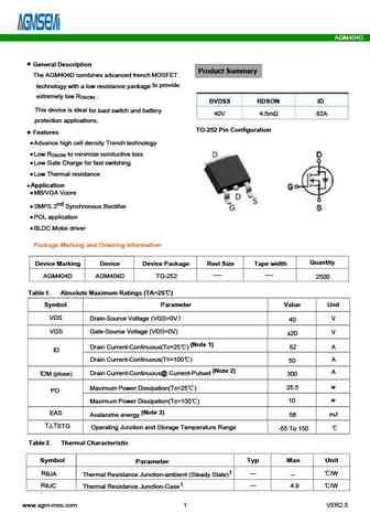
AGM404D GM General Description Product Summary The AGM404D combines advanced trench MOSFET to provide technology with a low resistance package extremely low R . DS(ON) BVDSS RDSON ID This device is ideal for load switch and battery 40V 4.5m 82A protection applications. TO-252 Pin Configuration Features Advance high cell density Trench technology Low R to mini... See More ⇒
agm405ap2.pdf

AGM405AP2 General Description Product Summary The AGM405AP2 combines advanced trench MOSFET to technology with a low resistance package provide extremely low R . DS(ON) BVDSS RDSON ID This device is ideal load switch and battery protection for 40V 4.4m 46A applications. PDFN3.3*3.3 Pin Configuration Features Advance high cell density Trench technology Low R t... See More ⇒
agm40p75a.pdf
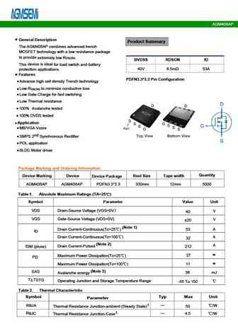
AGM40P75A General Description Product Summary The AGM40P75A combines advanced trench to MOSFET technology with a low resistance package provide extremely low R DS(ON) BVDSS RDSON ID This device is ideal for load switch and battery protection applications. -40V 7.0m -70A Features PDFN5*6 Pin Configuration Advance high cell density Trench technology Low R to minimize... See More ⇒
agm40p150c.pdf
AGM40P150C Table 2. P-Channel Electrical Characteristics (TJ=25 unless otherwisenoted) Symbol Parameter Conditions Min Typ Max Unit On/Off States BVDSS Drain-Source Breakdown Voltage VGS=0V ID=-250 A -40 -- -- V Zero Gate Voltage Drain Current V =-40V,V =0V -1 DS GS I -- -- A DSS Gate-Body Leakage Current V = 40V,V =0V 100 GS DS I -- -- nA GSS V Gate Threshold Voltage V =... See More ⇒
agm40p35d.pdf
AGM40P35D General Description Product Summary The AGM40P35D combines advanced trench MOSFET to provide technology with a low resistance package extremely low R DS(ON) BVDSS RDSON ID This device is ideal for load switch and battery protection applications. -40V 11m -60A Features Advance high cell density Trench technology TO-252 Pin Configuration Low R to minimize co... See More ⇒
agm4008ll.pdf
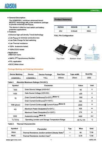
AGM4008LL General Description Product Summary The AGM4008LL combines advanced trench MOSFET technology with a low resistance package to provide extremely low R . DS(ON) BVDSS RDSON ID This device is ideal for load switch and battery protection applications. 40V 0.63m 500A Features Advance high cell density Trench technology TOLL Pin Configuration Low R to minim... See More ⇒
agm4025a.pdf
AGM4025A Typical Characteristics Fig.1 Typical Output Characteristics Fig.2 On-Resistance vs G-S Voltage Fig.3 Source Drain Forward Characteristics Fig.4 Gate-Charge Characteristics Fig.5 Normalized V vs T Fig.6 Normalized R vs T GS(th) J DSON J www.agm-mos.com 3 VER2.68 AGM4025A Fig.7 Capacitance Fig.8 Safe Operating Area 1 DUTY=0.5 0.2 0.1 0.1 0.05 0.02 PDM TON 0.01 ... See More ⇒
agm405mna.pdf
AGM405MNA Table 3. Electrical Characteristics (TJ=25 unless otherwise noted) Symbol Parameter Conditions Min Typ Max Unit On/Off States BV Drain-Source Breakdown Voltage V =0V I =250 A 40 -- -- V GS D DSS Zero Gate Voltage Drain Current V =40V,V =0V -- -- 1 A DS GS I DSS V = 20V,V =0V -- -- nA GS DS IGSS Gate-Body Leakage Current 100 VGS(th) Gate Threshold Voltage V... See More ⇒
agm406q.pdf
AGM406Q Table 3. Electrical Characteristics (TJ=25 unless otherwise noted) Symbol Parameter Conditions Min Typ Max Unit On/Off States BV Drain-Source Breakdown Voltage V =0V I =250 A 40 -- -- V GS D DSS Zero Gate Voltage Drain Current V =40V,V =0V -- -- 1 A DS GS I DSS Gate-Body Leakage Current V = 20V,V =0V -- -- nA GS DS I GSS 100 V Gate Threshold Voltage V =V ,I =... See More ⇒
agm403dg.pdf
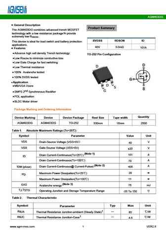
AGM403DG General Description Product Summary The AGM403DG combines advanced trench MOSFET to technology with a low resistance package provide extremely low R . DS(ON) BVDSS RDSON ID This device is ideal load switch and battery protection for applications. 40V 3.0m 101A Features Advance high cell density Trench technology TO-252 Pin Configuration Low R to min... See More ⇒
agm402a.pdf
AGM402A Table 3. Electrical Characteristics (TJ=25 unless otherwise noted) Symbol Parameter Conditions Min Typ Max Unit On/Off States BV Drain-Source Breakdown Voltage V =0V I =250 A 40 -- -- V GS D DSS Zero Gate Voltage Drain Current V =40V,V =0V -- -- 1 A DS GS I DSS V = 20V,V =0V -- -- nA GS DS IGSS Gate-Body Leakage Current 100 VGS(th) Gate Threshold Voltage V =... See More ⇒
agm40p30a.pdf
AGM40P30A Typical Characteristics -VDS,- Drain -Source Voltage (V) Tj - Junction Temperature ( C) Fig1. Typical Output Characteristics Fig2. -VGS(TH) Gate -Source Voltage Vs.Tj -VGS, -Gate -Source Voltage (V) Tj - Junction Temperature ( C) Fig3. Typical Transfer Characteristics Fig4. Normalized On-Resistance Vs. Tj -VSD, -Source-Drain Voltage (V) -VDS, -Drain -Source Voltage (V... See More ⇒
agm40p55a.pdf
AGM40P55A Typical Characteristics 80 80 VGS = -10V VGS = -3.5V VDS= -5V VGS = -4.5V 60 60 40 40 VGS = -3V 20 20 VGS = -2.5V 0 0 0 Drain-source voltage -VDS 4 5 1 2 3 0 1 2 3 (V) Gate-source voltage -VGS (V) 4 Figure 1. Output Characteristics Figure 2. Transfer Characteristics 10 80 ID= -16A 60 40 1 20 0 0.1 0 3 6 9 12 0.2 0.4 0.6 0.8 1.0 1.2 Gate-sourc... See More ⇒
agm403ap.pdf
AGM403AP N-Channel Typical Characteristics Fig.1 Typical Output Characteristics Fig.2 On-Resistance vs G-S Voltage Fig.3 Source Drain Forward Characteristics Fig.4 Gate-Charge Characteristics 1.8 1.8 1.4 1.4 1.0 1 0.6 0.6 0.2 0.2 -50 0 50 100 150 -50 0 50 100 150 TJ ,Junction Temperature ( ) TJ , Junction Temperature ( ) Fig.5 Normalized V vs T Fig.6 Normalized R vs T ... See More ⇒
agm40p100a.pdf
AGM40P100A Typical Electrical And Thermal Characteristics (Curves) Figure 1. Output Characteristics Figure 2. Transfer Characteristics Figure 3. Power Dissipation Figure 4. Drain Current Figure 5. BV vs Junction Temperature Figure 6. R vs Junction Temperature DSS DS(ON) www.agm-mos.com 3 VER2.69 AGM40P100A Figure 7. Gate Charge Waveforms Figure 8. Capacitance Figure 9. Body-... See More ⇒
agm40p100c.pdf
AGM40P100C Table 3. Electrical Characteristics (Tj=25 unless otherwise noted) Symbol Parameter Conditions Min Typ Max Unit On/Off States BVDSS Drain-Source Breakdown Voltage V =0V I =-250 A -40 -- -- V GS D Zero Gate Voltage Drain Current V =-40V,V =0V -- -- -1 A DS GS I DSS Gate-Body Leakage Current V = 20V,V =0V -- -- 100 nA GS DS I GSS VGS(th) Gate Threshold Voltage... See More ⇒
agm403a1-ku.pdf
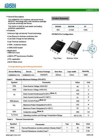
AGM403A1-KU General Description Product Summary The AGM403A1-KU combines advanced trench MOSFET technology with a low resistance package to provide extremely low R . DS(ON) device is ideal This for load switch and battery BVDSS RDSON ID protection applications. 40V 2.7m 120A Features Advance high cell density Trench technology PDFN5*6 Pin Configuration Low R t... See More ⇒
agm405q.pdf
AGM405Q Typical Characteristics Fig.1 Typical Output Characteristics Fig.2 On-Resistance vs. G-S Voltage Fig.3 Source Drain Forward Characteristics Fig.4 Gate-Charge Characteristics Fig.5 Normalized V vs. T Fig.6 Normalized R vs. T GS(th) J DSON J www.agm-mos.com 3 VER2.8 AGM405Q Fig.7 Capacitance Fig.8 Safe Operating Area 1 DUTY=0.5 0.3 0.1 0.1 0.05 PDM 0.02 TON T 0.... See More ⇒
agm40p35a-ku.pdf
AGM40P35A-KU General Description The AGM40P35A-KU combines advanced trench Product Summary to MOSFET technology with a low resistance package provide extremely low R DS(ON) This device is ideal for load switch and battery protection BVDSS RDSON ID applications. -40V 15m -60A Features Advance high cell density Trench technology PDFN5*6 Pin Configuration Low R to min... See More ⇒
agm40p25ap.pdf
AGM40P25AP Typical Electrical And Thermal Characteristics (Curves) Figure 1. Output Characteristics Figure 2. Transfer Characteristics Figure 3. Power Dissipation Figure 4. Drain Current Figure 5. BV vs Junction Temperature Figure 6. R vs Junction Temperature DSS DS(ON) www.agm-mos.com 3 VER2.7 AGM40P25AP Typical Electrical And Thermal Characteristics (Curves) Figure 7. Gat... See More ⇒
agm406mbp.pdf

AGM406MBP Typical Characteristics 2.7 40 10V,6V,5V,4.5V,4V IDS= 250uA 2.4 Max 2.1 30 VGS= 3.5V 1.8 Typ 1.5 20 1.2 Min 0.9 10 VGS= 3V Notes 0.6 1. 250 s pulse test 2. Tj=25 C 0.3 0 0 25 50 75 100 125 150 175 0 1 2 3 4 5 VDS, Drain -Source Voltage (V) Tj - Junction Temperature ( C) Fig1. Typical Output Characteristics Fig2. Typical V Gate -Source Voltage Vs. ... See More ⇒
agm40p26s.pdf
AGM40P26S General Description Product Summary The AGM40P26S combines advanced trench MOSFET to provide technology with a low resistance package extremely low R DS(ON) BVDSS RDSON ID This device is ideal and battery for load switch -40V 32m -6.0A protection applications. SOP8 Pin Configuration Features Advance high cell density Trench technology Low R to minimize co... See More ⇒
agm401a.pdf
AGM401A www.agm-mos.com 3 VER2.68 AGM401A www.agm-mos.com 5 VER2.68 AGM401A PDFN5*6 Marking Instructions Model1 Model2 www.agm-mos.com 7 VER2.68 AGM401A Disclaimer The information provided in this document is believed to be accurate and reliable. However,Shenzhen Core Control Source Electronics Technology Co., Ltd. does not assume any responsibility for the following c... See More ⇒
agm402q.pdf
AGM402Q Table 3. Electrical Characteristics (TJ=25 unless otherwise noted) Symbol Parameter Conditions Min Typ Max Unit On/Off States BV Drain-Source Breakdown Voltage V =0V I =250 A 40 -- -- V GS D DSS Zero Gate Voltage Drain Current V =40V,V =0V -- -- 1 A DS GS I DSS V = 20V,V =0V -- -- nA GS DS IGSS Gate-Body Leakage Current 100 VGS(th) Gate Threshold Voltage V =... See More ⇒
agm406mna.pdf
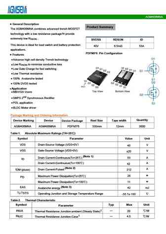
AGM406MNA Table 3. Electrical Characteristics (TJ=25 unless otherwise noted) Symbol Parameter Conditions Min Typ Max Unit On/Off States BV Drain-Source Breakdown Voltage V =0V I =250 A 40 -- -- V GS D DSS Zero Gate Voltage Drain Current V =40V,V =0V -- -- 1 A DS GS I DSS Gate-Body Leakage Current V = 20V,V =0V -- -- nA GS DS I GSS 100 V Gate Threshold Voltage V =V ,I... See More ⇒
Detailed specifications: AGM60P85AP, AGM60P85D, AGM60P85E, AGM60P90A, AGM60P90D, AGM610M, AGM610MN, AGM406Q, IRF520, AGM408MN, AGM409A, AGM409D, AGM40P100A, AGM40P100C, AGM40P100H, AGM40P13S, AGM40P150C
Keywords - AGM408M MOSFET specs
AGM408M cross reference
AGM408M equivalent finder
AGM408M pdf lookup
AGM408M substitution
AGM408M replacement
Can't find your MOSFET? Learn how to find a substitute transistor by analyzing voltage, current and package compatibility
🌐 : EN ES РУ

LIST
Last Update
MOSFET: AUB062N08BG | AUB060N08AG | AUB056N10 | AUB056N08BGL | AUB050N085 | AUB050N055 | AUB045N12 | AUB045N10BT | AUB039N10 | AUB034N10
Popular searches
2n408 | 2sc2690 | d718 datasheet | mp38 transistor | 2sc2389 | b331 transistor | 2sa720 | 2sc1345