View 3dd200 detailed specification:
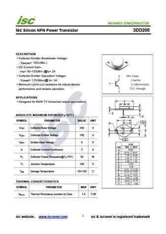
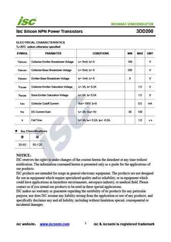
INCHANGE Semiconductor isc Silicon NPN Power Transistor 3DD200 DESCRIPTION Collector-Emitter Breakdown Voltage- V = 100V(Min.) (BR)CEO DC Current Gain- h = 30 120(Min.)@I = 2A FE C Collector-Emitter Saturation Voltage- V )= 1.5V(Max)@ I = 3A CE(sat C Minimum Lot-to-Lot variations for robust device performance and reliable operation APPLICATIONS Designed for B&W TV horizontal output applications. ABSOLUTE MAXIMUM RATINGS(T =25 ) a SYMBOL PARAMETER VALUE UNIT V Collector-Base Voltage 250 V CBO V Collector-Emitter Voltage 100 V CEO V Emitter-Base Voltage 6 V EBO I Collector Current-Continuous 3 A C P Collector Power Dissipation@T =75 30 W C C T Junction Temperature 150 J T Storage Temperature -55 150 stg THERMAL CHARACTERISTICS SYMBOL PARAMETER MAX UNIT Thermal Resistance,Junction to Case 1.5 /W R th j-c 1 isc website... See More ⇒
Keywords - ALL TRANSISTORS SPECS
3dd200.pdf Design, MOSFET, Power
3dd200.pdf RoHS Compliant, Service, Triacs, Semiconductor
3dd200.pdf Database, Innovation, IC, Electricity
BJT Parameters and How They Relate
🌐 : EN ES РУ

LIST
Last Update
BJT: ZDT6705 | GA1L4Z | GA1A4M | SBT42 | 2SA200-Y | 2SA200-O
Popular searches
irfz44n | irf3205 | irfz44n datasheet | 2n4401 | bc547 transistor | bd139 | 2n4401 datasheet