View pv501ba detailed specification:
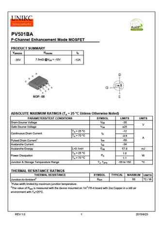
PV501BA P-Channel Enhancement Mode MOSFET PRODUCT SUMMARY V(BR)DSS RDS(ON) ID 7.5m @VGS = -10V -30V -12A SOP- 08 ABSOLUTE MAXIMUM RATINGS (TA = 25 C Unless Otherwise Noted) PARAMETERS/TEST CONDITIONS SYMBOL LIMITS UNITS VDS Drain-Source Voltage -30 V VGS Gate-Source Voltage 25 TA = 25 C -12 ID Continuous Drain Current TA = 70 C -9.6 A IDM -50 Pulsed Drain Current1 IAS Avalanche Current -34 EAS Avalanche Energy L=0.1mH 57.8 mJ TA = 25 C 1.8 PD Power Dissipation W TA = 70 C 1.1 TJ, TSTG Junction & Storage Temperature Range -55 to 150 C THERMAL RESISTANCE RATINGS THERMAL RESISTANCE SYMBOL TYPICAL MAXIMUM UNITS RqJA 68 C / W Junction-to-Ambient2 1 Pulse width limited by maximum junction temperature. 2 The value of RqJA is measured with the device mounted on 1in2 FR-4 board with 2oz.Copper.in a still air environment... See More ⇒
Keywords - ALL TRANSISTORS SPECS
pv501ba.pdf Design, MOSFET, Power
pv501ba.pdf RoHS Compliant, Service, Triacs, Semiconductor
pv501ba.pdf Database, Innovation, IC, Electricity
BJT Parameters and How They Relate
🌐 : EN ES РУ

LIST
Last Update
BJT: GA1A4M | SBT42 | 2SA200-Y | 2SA200-O | 2SD882-Q | 2SD882-P
Popular searches
irfz44n | irf3205 | irfz44n datasheet | 2n4401 | bc547 transistor | bd139 | 2n4401 datasheet