View mun5111dw detailed specification:
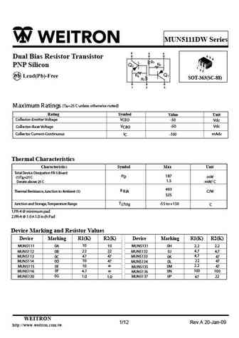
MUN5111DW Series 6 5 4 6 Dual Bias Resistor Transistor 5 4 R 1 R 2 PNP Silicon Q 2 1 2 3 R Q 2 1 SOT-363(SC-88) R 1 1 2 3 ( T =25 C unless otherwise noted) M aximum R atings A Rating Symbol Value Unit Collector-Emitter Voltage V -50 CEO Vdc Vdc Collector-Base Voltage VCBO -50 Collector Current-Continuous IC mAdc -100 Thermal Characteristics Characteristics Symbol Max Unit Total Device Dissipation FR-5 Board PD 187 mW (1)TA=25 C 1.5 Derate above 25 C mW/ C 493 R C/W Thermal Resistance, Junction to Ambient (1) JA 325 TJ,Tstg Junction and Storage, Temperature Range -55 to +150 C 1.FR-4 @ minimum pad 2.FR-4 @ 1.0 1.0 inch Pad Device Marking and Resistor Values Device Marking R1(K) R2(K) Device Marking R1(K) R2(K) 10 MUN5111 0A 10 MUN5131 0H 2.2 2.2 MUN5112 0B 22 22 4.7 MUN5132 0J 4.7 4.7 MUN5113 47 47 MUN5133 47 0C 0K 10 MUN... See More ⇒
Keywords - ALL TRANSISTORS SPECS
mun5111dw.pdf Design, MOSFET, Power
mun5111dw.pdf RoHS Compliant, Service, Triacs, Semiconductor
mun5111dw.pdf Database, Innovation, IC, Electricity
BJT Parameters and How They Relate
🌐 : EN ES РУ

LIST
Last Update
BJT: ZDT6705 | GA1L4Z | GA1A4M | SBT42 | 2SA200-Y | 2SA200-O
Popular searches
irfz44n | irf3205 | irfz44n datasheet | 2n4401 | bc547 transistor | bd139 | 2n4401 datasheet