APT4030CNR. Аналоги и основные параметры
Наименование производителя: APT4030CNR
Тип транзистора: MOSFET
Полярность: N
Предельные значения
Pd ⓘ - Максимальная рассеиваемая мощность: 150 W
|Vds|ⓘ - Максимально допустимое напряжение сток-исток: 400 V
|Vgs|ⓘ - Максимально допустимое напряжение затвор-исток: 30 V
|Id| ⓘ - Максимально допустимый постоянный ток стока: 15 A
Tj ⓘ - Максимальная температура канала: 150 °C
Электрические характеристики
tr ⓘ - Время нарастания: 23 ns
Cossⓘ - Выходная емкость: 385 pf
RDSonⓘ - Сопротивление сток-исток открытого транзистора: 0.3 Ohm
Тип корпуса: TO254
Аналог (замена) для APT4030CNR
- подборⓘ MOSFET транзистора по параметрам
APT4030CNR даташит
apt4030cnr.pdf

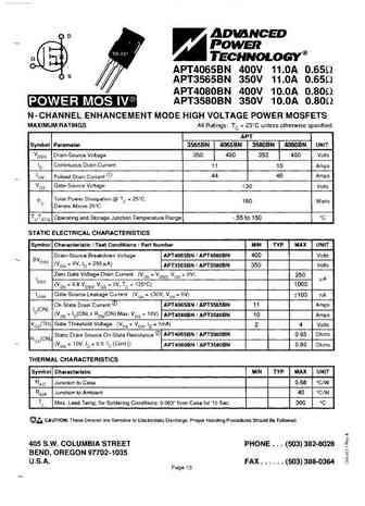
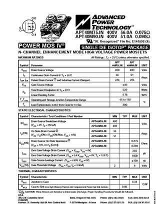
D TO-254 G S APT4030CNR 400V 15.0A 0.300 TM POWER MOS IV Avalanche Rated N - CHANNEL ENHANCEMENT MODE HIGH VOLTAGE POWER MOSFETS Faster Switching 100% Avalanche Tested Popular TO-254 Package Low Gate Charge Similar to the 2N7227, JX2N7227 and JV2N7227 MAXIMUM RATINGS All Ratings TC = 25 C unless otherwise specified. Symbol Parameter APT4030CNR UNIT VDSS Drai
apt4030.pdf
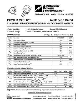
D TO-254 G S APT4030CNR 400V 15.0A 0.300 TM POWER MOS IV Avalanche Rated N - CHANNEL ENHANCEMENT MODE HIGH VOLTAGE POWER MOSFETS Faster Switching 100% Avalanche Tested Popular TO-254 Package Low Gate Charge Similar to the 2N7227, JX2N7227 and JV2N7227 MAXIMUM RATINGS All Ratings TC = 25 C unless otherwise specified. Symbol Parameter APT4030CNR UNIT VDSS Drai
apt40m42jn.pdf
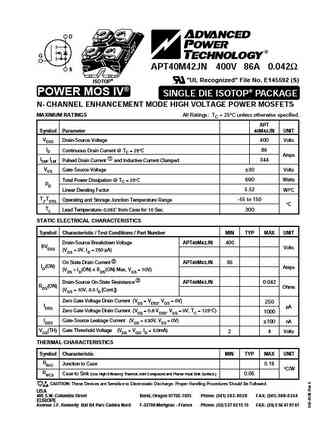
D G APT40M42JN 400V 86A 0.042 S "UL Recognized" File No. E145592 (S) ISOTOP POWER MOS IV SINGLE DIE ISOTOP PACKAGE N- CHANNEL ENHANCEMENT MODE HIGH VOLTAGE POWER MOSFETS MAXIMUM RATINGS All Ratings TC = 25 C unless otherwise specified. APT Symbol Parameter 40M42JN UNIT VDSS Drain-Source Voltage 400 Volts ID Continuous Drain Current @ TC = 25 C 86 Amps IDM, lLM Pulse
apt4012bvfrg apt4012svfrg.pdf
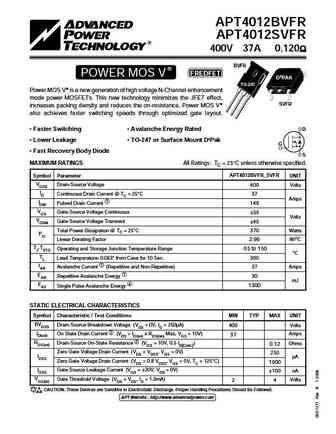
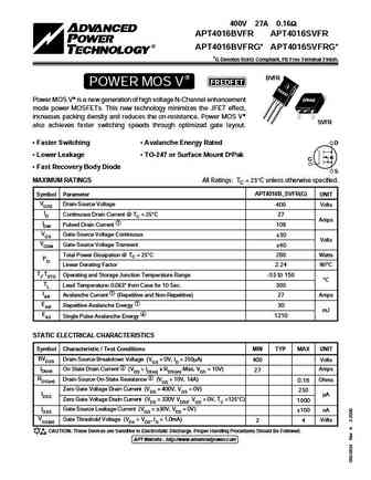
APT4012BVFR APT4012SVFR 400V 37A 0.120 BVFR FREDFET POWER MOS V D3PAK TO-247 Power MOS V is a new generation of high voltage N-Channel enhancement mode power MOSFETs. This new technology minimizes the JFET effect, SVFR increases packing density and reduces the on-resistance. Power MOS V also achieves faster switching speeds through optimized gate layout.
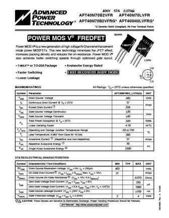
apt40m70lvr.pdf
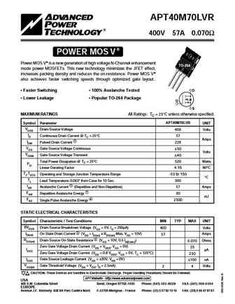
APT40M70LVR 400V 57A 0.070 POWER MOS V Power MOS V is a new generation of high voltage N-Channel enhancement TO-264 mode power MOSFETs. This new technology minimizes the JFET effect, increases packing density and reduces the on-resistance. Power MOS V also achieves faster switching speeds through optimized gate layout.. Faster Switching 100% Avalanche Tested D Lowe
apt4016bn.pdf

D TO-247 G APT4016BN 400V 31.0A 0.16 S APT4018BN 400V 29.0A 0.18 POWER MOS IV N- CHANNEL ENHANCEMENT MODE HIGH VOLTAGE POWER MOSFETS MAXIMUM RATINGS All Ratings TC = 25 C unless otherwise specified. APT APT Symbol Parameter 4016BN 4018BN UNIT VDSS Drain-Source Voltage 400 400 Volts ID Continuous Drain Current @ TC = 25 C 31 29 Amps IDM Pulsed Drain Current 1 124 116
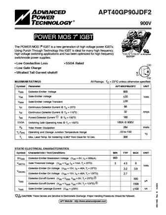
apt40gp90j.pdf

TYPICAL PERFORMANCE CURVES APT40GP90J APT40GP90J 900V POWER MOS 7 IGBT The POWER MOS 7 IGBT is a new generation of high voltage power IGBTs. Using Punch Through Technology this IGBT is ideal for many high frequency, "UL Recognized" high voltage switching applications and has been optimized for high frequency ISOTOP switchmode power supplies. Low Conduction Loss SSOA Rat
apt40gp60b2df2.pdf
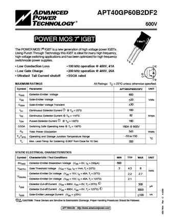
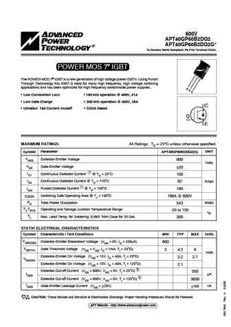
TYPICAL PERFORMANCE CURVES APT40GP60B2DF2 APT40GP60B2DF2 600V POWER MOS 7 IGBT TM T-Max The POWER MOS 7 IGBT is a new generation of high voltage power IGBTs. Using Punch Through Technology this IGBT is ideal for many high frequency, high voltage switching applications and has been optimized for high frequency G switchmode power supplies. C E Low Conduction Loss 100 k
apt40gp90b2dq2g.pdf
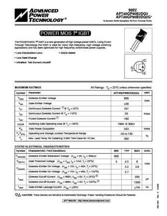
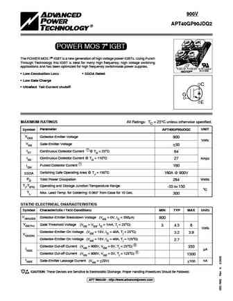
TYPICAL PERFORMANCE CURVES APT40GP90B2DQ2(G) 900V APT40GP90B2DQ2 APT40GP90B2DQ2G* *G Denotes RoHS Compliant, Pb Free Terminal Finish. POWER MOS 7 IGBT T-Max The POWER MOS 7 IGBT is a new generation of high voltage power IGBTs. Using Punch Through Technology this IGBT is ideal for many high frequency, high voltage switching applications and has been optimized for high f

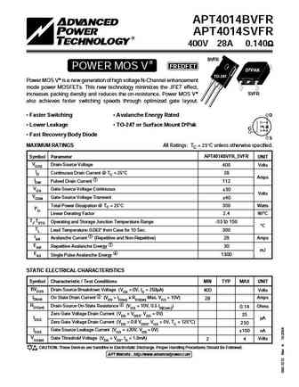
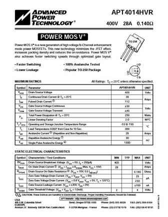
apt4014bvr.pdf
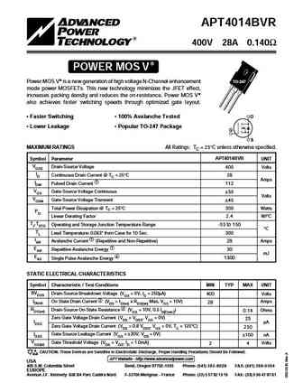
APT4014BVR 400V 28A 0.140 POWER MOS V Power MOS V is a new generation of high voltage N-Channel enhancement TO-247 mode power MOSFETs. This new technology minimizes the JFET effect, increases packing density and reduces the on-resistance. Power MOS V also achieves faster switching speeds through optimized gate layout. Faster Switching 100% Avalanche Tested D Lower L
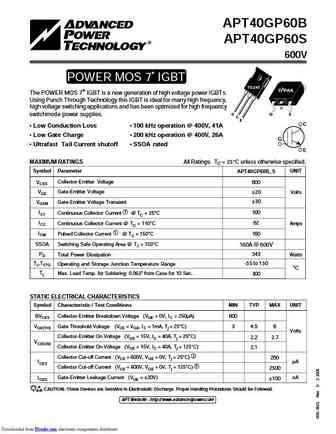
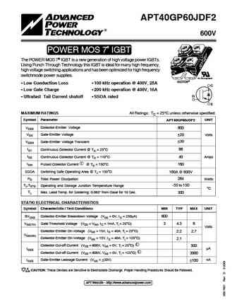
apt40gp60b.pdf
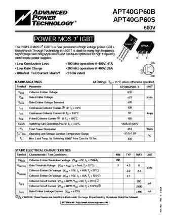
APT40GP60B APT40GP60S 600V POWER MOS 7 IGBT TO-247 D3PAK The POWER MOS 7 IGBT is a new generation of high voltage power IGBTs. Using Punch Through Technology this IGBT is ideal for many high frequency, high voltage switching applications and has been optimized for high frequency C G G E switchmode power supplies. C E C Low Conduction Loss 100 kHz operation @ 400V, 4
apt4018bn.pdf

D TO-247 G APT4016BN 400V 31.0A 0.16 S APT4018BN 400V 29.0A 0.18 POWER MOS IV N- CHANNEL ENHANCEMENT MODE HIGH VOLTAGE POWER MOSFETS MAXIMUM RATINGS All Ratings TC = 25 C unless otherwise specified. APT APT Symbol Parameter 4016BN 4018BN UNIT VDSS Drain-Source Voltage 400 400 Volts ID Continuous Drain Current @ TC = 25 C 31 29 Amps IDM Pulsed Drain Current 1 124 116
apt40gp90b2df2.pdf
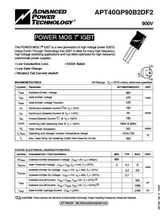
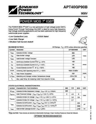
TYPICAL PERFORMANCE CURVES APT40GP90B2DF2 APT40GP90B2DF2 900V POWER MOS 7 IGBT T-MaxTM The POWER MOS 7 IGBT is a new generation of high voltage power IGBTs. Using Punch Through Technology this IGBT is ideal for many high frequency, high voltage switching applications and has been optimized for high frequency switchmode power supplies. G C E Low Conduction Loss SSOA R
apt40gf120jrd.pdf
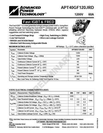
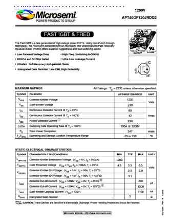
APT40GF120JRD 1200V 60A Fast IGBT & FRED The Fast IGBT is a new generation of high voltage power IGBTs. Using Non- Punch Through Technology the Fast IGBT combined with an APT free- wheeling ultraFast Recovery Epitaxial Diode (FRED) offers superior ruggedness and fast switching speed. "UL Recognized" ISOTOP Low Forward Voltage Drop High Freq. Switching to 20KHz C L
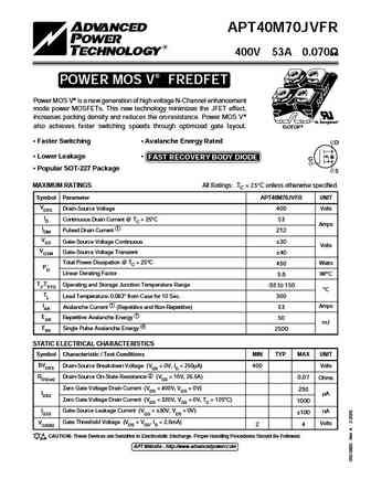
apt40m70jvr.pdf
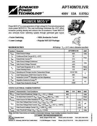
APT40M70JVR 400V 53A 0.070 POWER MOS V Power MOS V is a new generation of high voltage N-Channel enhancement mode power MOSFETs. This new technology minimizes the JFET effect, increases packing density and reduces the on-resistance. Power MOS V also achieves faster switching speeds through optimized gate layout. "UL Recognized" ISOTOP Faster Switching 100% Avalanche
apt4018hvr.pdf
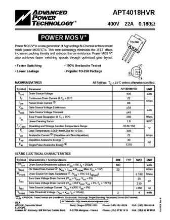
APT4018HVR 400V 22A 0.180 POWER MOS V TO-258 Power MOS V is a new generation of high voltage N-Channel enhancement mode power MOSFETs. This new technology minimizes the JFET effect, increases packing density and reduces the on-resistance. Power MOS V also achieves faster switching speeds through optimized gate layout. D Faster Switching 100% Avalanche Tested Lower
apt4016bvr.pdf

APT4016BVR 400V 27A 0.160 POWER MOS V Power MOS V is a new generation of high voltage N-Channel enhancement TO-247 mode power MOSFETs. This new technology minimizes the JFET effect, increases packing density and reduces the on-resistance. Power MOS V also achieves faster switching speeds through optimized gate layout. D Faster Switching 100% Avalanche Tested Lower
apt40m35jvr.pdf

APT40M35JVR 400V 93A 0.035 POWER MOS V Power MOS V is a new generation of high voltage N-Channel enhancement mode power MOSFETs. This new technology minimizes the JFET effect, increases packing density and reduces the on-resistance. Power MOS V also achieves faster switching speeds through optimized gate layout. "UL Recognized" ISOTOP Faster Switching 100% Avalanche
apt40gp60j.pdf
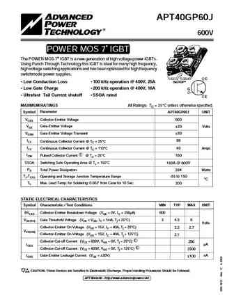
APT40GP60J 600V POWER MOS 7 IGBT The POWER MOS 7 IGBT is a new generation of high voltage power IGBTs. Using Punch Through Technology this IGBT is ideal for many high frequency, high voltage switching applications and has been optimized for high frequency switchmode power supplies. "UL Recognized" C Low Conduction Loss 100 kHz operation @ 400V, 25A ISOTOP Low Gate
apt40gp90jdq2.pdf
TYPICAL PERFORMANCE CURVES APT40GP90JDQ2 900V APT40GP90JDQ2 POWER MOS 7 IGBT The POWER MOS 7 IGBT is a new generation of high voltage power IGBTs. Using Punch Through Technology this IGBT is ideal for many high frequency, high voltage switching applications and has been optimized for high frequency switchmode power supplies. "UL Recognized" ISOTOP file # E145592 Low
apt40m75jn.pdf
D G APT40M75JN 400V 56.0A 0.075 S APT40M90JN 400V 51.0A 0.090 ISOTOP "UL Recognized" File No. E145592 (S) POWER MOS IV SINGLE DIE ISOTOP PACKAGE N- CHANNEL ENHANCEMENT MODE HIGH VOLTAGE POWER MOSFETS MAXIMUM RATINGS All Ratings TC = 25 C unless otherwise specified. APT APT Symbol Parameter 40M75JN 40M90JN UNIT VDSS Drain-Source Voltage 400 400 Volts ID Continuous Dr
apt4014bvfrg apt4014svfrg.pdf
APT4014BVFR APT4014SVFR 400V 28A 0.140 BVFR FREDFET POWER MOS V D3PAK TO-247 Power MOS V is a new generation of high voltage N-Channel enhancement mode power MOSFETs. This new technology minimizes the JFET effect, SVFR increases packing density and reduces the on-resistance. Power MOS V also achieves faster switching speeds through optimized gate layout.
apt40gp60bg.pdf

APT40GP60B APT40GP60S 600V POWER MOS 7 IGBT TO-247 D3PAK The POWER MOS 7 IGBT is a new generation of high voltage power IGBTs. Using Punch Through Technology this IGBT is ideal for many high frequency, high voltage switching applications and has been optimized for high frequency C G G E switchmode power supplies. C E C Low Conduction Loss 100 kHz operation @ 400V, 4
apt40gp60sg.pdf
APT40GP60B APT40GP60S 600V POWER MOS 7 IGBT TO-247 D3PAK The POWER MOS 7 IGBT is a new generation of high voltage power IGBTs. Using Punch Through Technology this IGBT is ideal for many high frequency, high voltage switching applications and has been optimized for high frequency C G G E switchmode power supplies. C E C Low Conduction Loss 100 kHz operation @ 400V, 4
apt40gp90jdf2.pdf
TYPICAL PERFORMANCE CURVES APT40GP90JDF2 APT40GP90JDF2 900V POWER MOS 7 IGBT The POWER MOS 7 IGBT is a new generation of high voltage power IGBTs. Using Punch Through Technology this IGBT is ideal for many high frequency, "UL Recognized" high voltage switching applications and has been optimized for high frequency ISOTOP switchmode power supplies. Low Conduction Loss SS
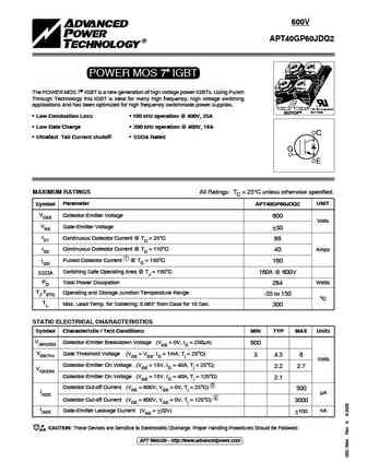
apt4020bvfrg.pdf
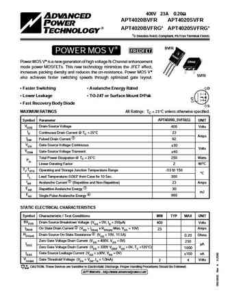
400V 23A 0.20 APT4020BVFR APT4020SVFR APT4020BVFRG* APT4020SVFRG* *G Denotes RoHS Compliant, Pb Free Terminal Finish. BVFR FREDFET POWER MOS V Power MOS V is a new generation of high voltage N-Channel enhancement D3PAK mode power MOSFETs. This new technology minimizes the JFET effect, increases packing density and reduces the on-resistance. Power MOS V SVF
apt40m82wvr.pdf
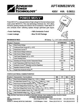
APT40M82WVR 400V 44A 0.082 POWER MOS V TO-267 Power MOS V is a new generation of high voltage N-Channel enhancement mode power MOSFETs. This new technology minimizes the JFET effect, increases packing density and reduces the on-resistance. Power MOS V also achieves faster switching speeds through optimized gate layout. Faster Switching 100% Avalanche Tested D Lower
apt4020.pdf
D TO-247 G APT4020BN 400V 26.0A 0.20 S APT4025BN 400V 23.0A 0.25 POWER MOS IV N- CHANNEL ENHANCEMENT MODE HIGH VOLTAGE POWER MOSFETS MAXIMUM RATINGS All Ratings TC = 25 C unless otherwise specified. APT APT Symbol Parameter 4020BN 4025BN UNIT VDSS Drain-Source Voltage 400 400 Volts ID Continuous Drain Current @ TC = 25 C 26 23 Amps IDM Pulsed Drain Current 1 104 92
apt40m70jvfr.pdf
APT40M70JVFR 400V 53A 0.070 POWER MOS V FREDFET Power MOS V is a new generation of high voltage N-Channel enhancement mode power MOSFETs. This new technology minimizes the JFET effect, increases packing density and reduces the on-resistance. Power MOS V "UL Recognized" also achieves faster switching speeds through optimized gate layout. ISOTOP Faster
apt40gp60jdq2.pdf
TYPICAL PERFORMANCE CURVES APT40GP60JDQ2 600V APT40GP60JDQ2 POWER MOS 7 IGBT The POWER MOS 7 IGBT is a new generation of high voltage power IGBTs. Using Punch Through Technology this IGBT is ideal for many high frequency, high voltage switching applications and has been optimized for high frequency switchmode power supplies. "UL Recongnized" ISOTOP file # 145592 Low
apt4020bvr.pdf
APT4020BVR 400V 23A 0.200 POWER MOS V Power MOS V is a new generation of high voltage N-Channel enhancement TO-247 mode power MOSFETs. This new technology minimizes the JFET effect, increases packing density and reduces the on-resistance. Power MOS V also achieves faster switching speeds through optimized gate layout. D Faster Switching 100% Avalanche Tested Lower
apt40gp60jdf2.pdf
TYPICAL PERFORMANCE CURVES APT40GP60JDF2 APT40GP60JDF2 600V POWER MOS 7 IGBT The POWER MOS 7 IGBT is a new generation of high voltage power IGBTs. Using Punch Through Technology this IGBT is ideal for many high frequency, high voltage switching applications and has been optimized for high frequency switchmode power supplies. "UL Recognized" ISOTOPfi Low Conduction Loss
apt4020bn.pdf

D TO-247 G APT4020BN 400V 26.0A 0.20 S APT4025BN 400V 23.0A 0.25 POWER MOS IV N- CHANNEL ENHANCEMENT MODE HIGH VOLTAGE POWER MOSFETS MAXIMUM RATINGS All Ratings TC = 25 C unless otherwise specified. APT APT Symbol Parameter 4020BN 4025BN UNIT VDSS Drain-Source Voltage 400 400 Volts ID Continuous Drain Current @ TC = 25 C 26 23 Amps IDM Pulsed Drain Current 1 104 92
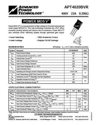
apt40m35pvr.pdf
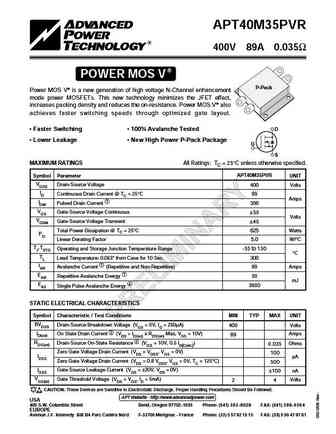
APT40M35PVR 400V 89A 0.035 POWER MOS V P-Pack Power MOS V is a new generation of high voltage N-Channel enhancement mode power MOSFETs. This new technology minimizes the JFET effect, increases packing density and reduces the on-resistance. Power MOS V also achieves faster switching speeds through optimized gate layout. Faster Switching 100% Avalanche Tested D Lower
apt40m70b2vfrg apt40m70lvfrg.pdf
400V 57A 0.070 APT40M70B2VFR APT40M70LVFR APT40M70B2VFRG* APT40M40LVFRG* *G Denotes RoHS Compliant, Pb Free Terminal Finish. B2VFR POWER MOS V FREDFET T-MAX Power MOS V is a new generation of high voltage N-Channel enhancement TO-264 mode power MOSFETs. This new technology minimizes the JFET effect, increases packing density and reduces the on-resistance
apt4012bvr.pdf

APT4012BVR 400V 37A 0.120 POWER MOS V Power MOS V is a new generation of high voltage N-Channel enhancement TO-247 mode power MOSFETs. This new technology minimizes the JFET effect, increases packing density and reduces the on-resistance. Power MOS V also achieves faster switching speeds through optimized gate layout. Faster Switching 100% Avalanche Tested D Lower L
apt40gt60br.pdf
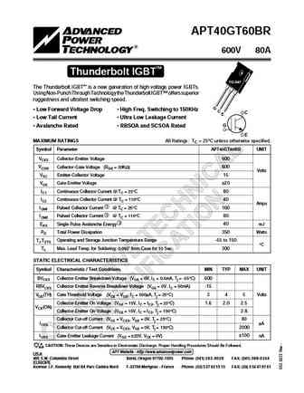
APT40GT60BR 600V 80A Thunderbolt IGBT TO-247 The Thunderbolt IGBT is a new generation of high voltage power IGBTs. Using Non-Punch Through Technology the Thunderbolt IGBT offers superior ruggedness and ultrafast switching speed. G Low Forward Voltage Drop High Freq. Switching to 150KHz C C E Low Tail Current Ultra Low Leakage Current Avalanche Rated
apt4015avr.pdf
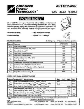
APT4015AVR 400V 25.5A 0.150 POWER MOS V TO-3 Power MOS V is a new generation of high voltage N-Channel enhancement mode power MOSFETs. This new technology minimizes the JFET effect, increases packing density and reduces the on-resistance. Power MOS V also achieves faster switching speeds through optimized gate layout. D Faster Switching 100% Avalanche Tested Lower
apt4014hvr.pdf
APT4014HVR 400V 28A 0.140 POWER MOS V TO-258 Power MOS V is a new generation of high voltage N-Channel enhancement mode power MOSFETs. This new technology minimizes the JFET effect, increases packing density and reduces the on-resistance. Power MOS V also achieves faster switching speeds through optimized gate layout. Faster Switching 100% Avalanche Tested D Lower
apt4016bvfrg apt4016svfrg.pdf
400V 27A 0.16 APT4016BVFR APT4016SVFR APT4016BVFRG* APT4016SVFRG* *G Denotes RoHS Compliant, Pb Free Terminal Finish. BVFR FREDFET POWER MOS V Power MOS V is a new generation of high voltage N-Channel enhancement D3PAK mode power MOSFETs. This new technology minimizes the JFET effect, increases packing density and reduces the on-resistance. Power MOS V SVF
apt40gp60b2dq2g.pdf
TYPICAL PERFORMANCE CURVES APT40GP60B2DQ2(G) 600V APT40GP60B2DQ2 APT40GP60B2DQ2G* *G Denotes RoHS Compliant, Pb Free Terminal Finish. POWER MOS 7 IGBT TM T-Max The POWER MOS 7 IGBT is a new generation of high voltage power IGBTs. Using Punch Through Technology this IGBT is ideal for many high frequency, high voltage switching applications and has been optimized for high
apt40gf120jrdq2.pdf
APT40GF120JRDQ2 TYPICAL PERFORMANCE CURVES APT40GF120JRDQ2 1200V APT40GF120JRDQ2 FAST IGBT & FRED The Fast IGBT is a new generation of high voltage power IGBTs. Using Non-Punch through technology, the Fast IGBT combined with an Microsemi free wheeling Ultra Fast Recovery Epitaxial Diode (FRED) offers superior ruggedness and fast switching speed. "UL Recognized" ISOTO
apt40gr120s.pdf

APT40GR120B_S APT40GR120B APT40GR120S 1200V, 40A, VCE(on)= 2.5V Typical . Ultra Fast NPT - IGBT (B) The Ultra Fast NPT - IGBT is a new generation of high voltage power IGBTs. D3PA K Using Non-Punch-Through Technology, the Ultra Fast NPT-IGBT offers superior ruggedness and ultrafast switching speed. (S) C G E Features G C Low Saturation Voltage Short Circuit
apt40n60b2cf apt40n60lcf.pdf
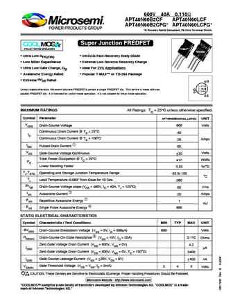
FINAL DATA SHEET 600V 40A 0.110 APT40N60B2CF APT40N60LCF APT40N60B2CFG* APT40N60LCFG* *G Denotes RoHS Compliant, Pb Free Terminal Finish. Super Junction FREDFET COOLMOS TM Power Semiconductors T-Max TO-264 Ultra Low RDS(ON) Intrinsic Fast-Recovery Body Diode Low Miller Capacitance Extreme Low Reverse Recovery Charge Ultra Low Gate Charge, Qg Ideal
apt40gr120b.pdf
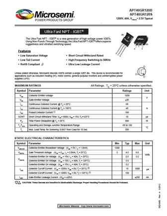
APT40GR120B_S APT40GR120B APT40GR120S 1200V, 40A, VCE(on)= 2.5V Typical . Ultra Fast NPT - IGBT (B) The Ultra Fast NPT - IGBT is a new generation of high voltage power IGBTs. D3PA K Using Non-Punch-Through Technology, the Ultra Fast NPT-IGBT offers superior ruggedness and ultrafast switching speed. (S) C G E Features G C Low Saturation Voltage Short Circuit
apt40gt60brg.pdf
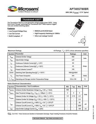
APT40GT60BR 600V, 80A, VCE(ON) = 2.1V Typical Thunderbolt IGBT The Thunderbolt IGBT is a new generation of high voltage power IGBTs. Using Non-Punch-Through Technology, the Thunderbolt IGBT offers superior rugged- ness and ultrafast switching speed. Features RBSOA and SCSOA Rated Low Forward Voltage Drop High Frequency Switching to 150KHz Low Tail Current G
apt40m35jvfr.pdf
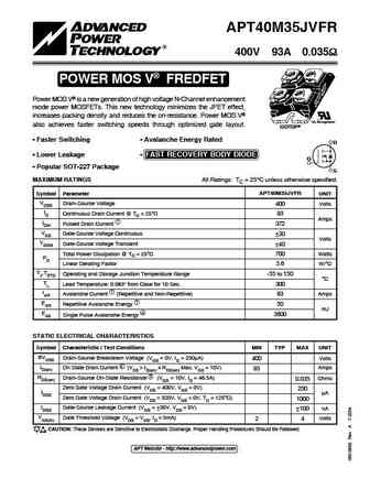
APT40M35JVFR 400V 93A 0.035 POWER MOS V FREDFET Power MOS V is a new generation of high voltage N-Channel enhancement mode power MOSFETs. This new technology minimizes the JFET effect, increases packing density and reduces the on-resistance. Power MOS V "UL Recognized" also achieves faster switching speeds through optimized gate layout. ISOTOP Faster
apt4020bvfr.pdf
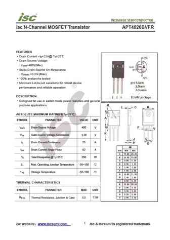
isc N-Channel MOSFET Transistor APT4020BVFR FEATURES Drain Current I =23A@ T =25 D C Drain Source Voltage- V =400V(Min) DSS Static Drain-Source On-Resistance R =0.2 (Max) DS(on) 100% avalanche tested Minimum Lot-to-Lot variations for robust device performance and reliable operation DESCRIPTION Designed for use in switch mode power supplies and general purpo
apt4014bvfr.pdf

isc N-Channel MOSFET Transistor APT4014BVFR FEATURES Drain Current I = 28A@ T =25 D C Drain Source Voltage- V =400V(Min) DSS Static Drain-Source On-Resistance R =0.14 (Max) DS(on) 100% avalanche tested Minimum Lot-to-Lot variations for robust device performance and reliable operation DESCRIPTION Designed for use in switch mode power supplies and general pur
Другие IGBT... APT4014BVR, APT4014HVR, APT4015AVR, APT4016BN, APT4016BVR, APT4018HVR, APT4020BN, APT4020BVR, 7N65, APT40M35JVR, APT40M35PVR, APT40M42JN, APT40M70JVR, APT40M70LVR, APT40M75JN, APT40M82WVR, APT5010B2VFR
🌐 : EN ES РУ

Список транзисторов
Обновления
MOSFET: AUW033N08BG | AUW025N10 | AUR030N10 | AUR020N10 | AUR020N085 | AUR014N10 | AUP074N10 | AUP065N10 | AUP062N08BG | AUP060N08AG | HYG053N10NS1B | HYG053N10NS1P | AP220N04T | AP220N04P | QM3126M3 | AUP060N055
Popular searches
bc550c | 2n3904 transistor datasheet | p75nf75 | d880 transistor | 2sc1845 | p60nf06 | 2sa1837 | ksc1845 transistor