IPB035N08N3G. Аналоги и основные параметры
Наименование производителя: IPB035N08N3G
Тип транзистора: MOSFET
Полярность: N
Предельные значения
Pd ⓘ
- Максимальная рассеиваемая мощность: 214 W
|Vds|ⓘ - Максимально допустимое напряжение сток-исток: 80 V
|Vgs|ⓘ - Максимально допустимое напряжение затвор-исток: 20 V
|Id| ⓘ - Максимально допустимый постоянный ток стока: 100 A
Tj ⓘ - Максимальная температура канала: 175 °C
Электрические характеристики
tr ⓘ -
Время нарастания: 79 ns
Cossⓘ - Выходная емкость: 1640 pf
RDSonⓘ - Сопротивление сток-исток открытого транзистора: 0.00375 Ohm
Тип корпуса: TO263
Аналог (замена) для IPB035N08N3G
- подборⓘ MOSFET транзистора по параметрам
IPB035N08N3G даташит
..1. Size:1018K infineon
ipp037n08n3ge8181 ipp037n08n3g ipi037n08n3g ipb035n08n3g.pdf 
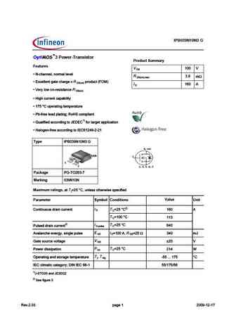
IPP037N08N3 G IPI037N08N3 G IPB035N08N3 G 3 Power-Transistor Product Summary Features V D Q #4513I CG9D389>7 1>4 CI>3 B53 R m D n) m x Q ( @D9=9J54 D538>?F5BD5BC I 1 D Q H3579>55B9>7 3?45 Q .5BI B5C9CD1>35 + D n) #) ' ' ! Q ' 381>>5?B=1
..2. Size:494K infineon
ipp037n08n3g ipi037n08n3g ipb035n08n3g.pdf 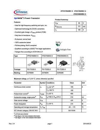
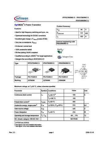
IPP037N08N3 G IPI037N08N3 G IPB035N08N3 G OptiMOS 3 Power-Transistor Product Summary Features V 80 V DS Ideal for high frequency switching and sync. rec. R 3.5 m DS(on),max Optimized technology for DC/DC converters I 100 A D Excellent gate charge x R product (FOM) DS(on) Very low on-resistance RDS(on) N-channel, normal level 100% avalanche tested
..3. Size:228K inchange semiconductor
ipb035n08n3g.pdf 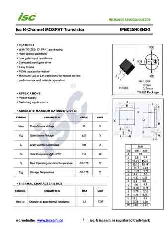
Isc N-Channel MOSFET Transistor IPB035N08N3G FEATURES With TO-263( D PAK ) packaging High speed switching Low gate input resistance Standard level gate drive Easy to use 100% avalanche tested Minimum Lot-to-Lot variations for robust device performance and reliable operation APPLICATIONS Power supply Switching applications ABSOLUTE MAXIMUM RATINGS(T =25 )
9.1. Size:475K infineon
ipb034n06l3g ipi037n06l3g ipp037n06l3g.pdf 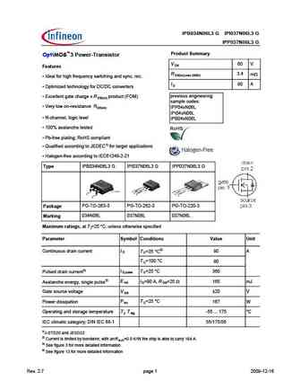
Type IPB034N06L3 G IPI037N06L3 G IPP037N06L3 G Product Summary OptiMOS 3 Power-Transistor V 60 V DS Features R 3.4 m DS(on),max (SMD) Ideal for high frequency switching and sync. rec. I 90 A D Optimized technology for DC/DC converters previous engineering Excellent gate charge x R product (FOM) DS(on) sample codes Very low on-resistance RDS(on) IPP04xN06
9.2. Size:674K infineon
ipb034n06n3.pdf 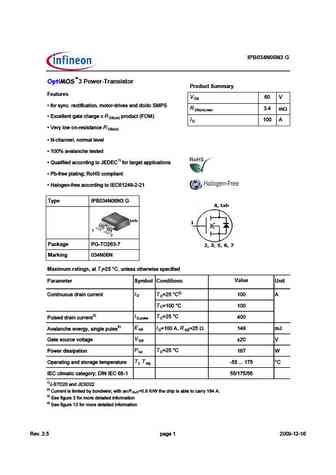
pe IPB034N06N3 G 3 Power-Transistor Product Summary Features V D P 6?A BH>3 A53C96931C9?> =?C?A 4A9E5B 1>4 43 43 ,&), R 4 m D n) m x P G35
9.3. Size:696K infineon
ipb030n08n3.pdf 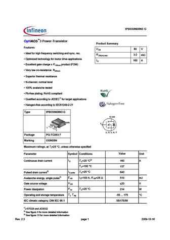
IPB030N08N3 G 3 Power-Transistor Product Summary Features V D Q #4513I CG9D389>7 1>4 CI>3 B53 R m D n) m x Q ( @D9=9J54 D538>?C I 1 D Q H35
9.4. Size:264K infineon
ipp039n04lg ipb039n04lg.pdf 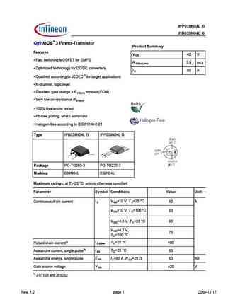
Type IPP039N04L G IPB039N04L G OptiMOS 3 Power-Transistor Product Summary Features V 40 V DS Fast switching MOSFET for SMPS R 3.9 m DS(on),max Optimized technology for DC/DC converters I 80 A D Qualified according to JEDEC1) for target applications N-channel, logic level Excellent gate charge x R product (FOM) DS(on) Very low on-resistance R DS(on
9.5. Size:484K infineon
ipb037n06n3g ipi040n06n3g ipp040n06n3g.pdf 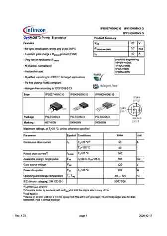
Type IPB037N06N3 G IPI040N06N3 G IPP040N06N3 G OptiMOS 3 Power-Transistor Product Summary Features V 60 V DS R 3.7 for sync. rectification, drives and dc/dc SMPS m DS(on),max (SMD) I 90 A Excellent gate charge x R product (FOM) D DS(on) previous engineering Very low on-resistance R DS(on) sample codes N-channel, normal level IPP04xN06N IPI04xN06N Ava
9.6. Size:1003K infineon
ipb033n10n5lf.pdf 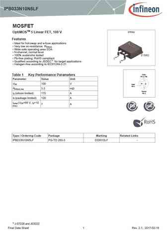
IPB033N10N5LF MOSFET D PAK OptiMOSTM 5 Linear FET, 100 V Features Ideal for hot-swap and e-fuse applications Very low on-resistance R DS(on) Wide safe operating area SOA N-channel, normal level 100% avalanche tested Pb-free plating; RoHS compliant Qualified according to JEDEC1) for target applications Halogen-free according to IEC61249-2-21 Drain
9.7. Size:508K infineon
ipb038n12n3-g ipi041n12n3-g ipp041n12n3-g.pdf 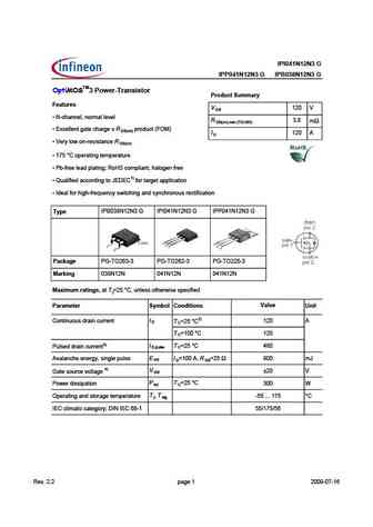
IPI041N12N3 G IPP041N12N3 G IPB038N12N3 G OptiMOSTM3 Power-Transistor Product Summary Features V 120 V DS N-channel, normal level R 3.8 m DS(on),max (TO-263) Excellent gate charge x R product (FOM) DS(on) I 120 A D Very low on-resistance R DS(on) 175 C operating temperature Pb-free lead plating; RoHS compliant, halogen free Qualified according to
9.8. Size:534K infineon
ipb031ne7n3 ipb031ne7n3g.pdf 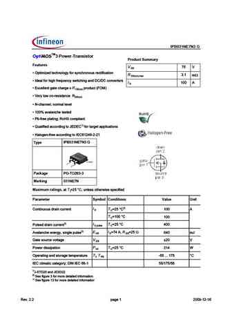
IPB031NE7N3 G TM 3 Power-Transistor Product Summary Features V 7 D Q ( @D9=9J54 D538>??EC B53D96931D9?> R 1 m D n) m x Q #4513I CG9D389>7 1>4 3?>F5BD5BC I 1 D Q H35
9.9. Size:344K infineon
ipb039n04l-g ipp039n04l-g.pdf 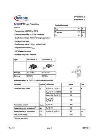
Type IPP039N04L G IPB039N04L G OptiMOS 3 Power-Transistor Product Summary Features V 40 V DS Fast switching MOSFET for SMPS R 3.9 m DS(on),max Optimized technology for DC/DC converters I 80 A D Qualified according to JEDEC1) for target applications N-channel, logic level Excellent gate charge x R product (FOM) DS(on) Very low on-resistance R DS(on
9.10. Size:664K infineon
ipb039n10n3ge8187.pdf 
IPB039N10N3 G 3 Power-Transistor Product Summary Features V 1 D P ' 381>>5?A=1
9.11. Size:279K infineon
ipb03n03lbg.pdf 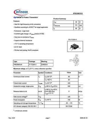
IPB03N03LB OptiMOS 2 Power-Transistor Product Summary Features V 30 V DS Ideal for high-frequency dc/dc converters R 2.8 m DS(on),max Qualified according to JEDEC1) for target application I 80 A D N-channel - Logic level Excellent gate charge x R product (FOM) DS(on) Very low on-resistance R DS(on) PG-TO220-3-1 PG-TO263-3 Superior thermal resistan
9.12. Size:633K infineon
ipb036n12n3g.pdf 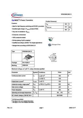
IPB036N12N3 G 3 Power-Transistor Product Summary Features V 1 D Q #4513I CG9D389>7 1>4 3?>F5BD5BC R m D n) m x Q H35
9.13. Size:615K infineon
ipb039n04l .pdf 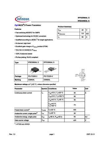
pe %% # ! % # ! % (>.;?6?@ %>E Features 4 D S 4EF EI
9.14. Size:1124K infineon
ipb031n08n5.pdf 
MOSFET Metal Oxide Semiconductor Field Effect Transistor OptiMOSTM OptiMOS 5 Power-Transistor, 80 V IPB031N08N5 Data Sheet Rev. 2.0 Final Power Management & Multimarket OptiMOS 5 Power-Transistor, 80 V IPB031N08N5 D PAK 1 Description Features Ideal for high frequency switching and sync. rec. Excellent gate charge x R product (FOM) DS(on) Very low on-resistance R
9.15. Size:725K infineon
ipp034n03lg ipb034n03lg.pdf 
Type IPP034N03L G IPB034N03L G 3 Power-Transistor Product Summary Features V 30 V DS Fast switching MOSFET for SMPS R 3.4 mW DS(on),max Optimized technology for DC/DC converters I 80 A D Qualified according to JEDEC1) for target applications N-channel, logic level Excellent gate charge x R product (FOM) DS(on) Very low on-resistance R DS(on)
9.16. Size:686K infineon
ipb039n04l.pdf 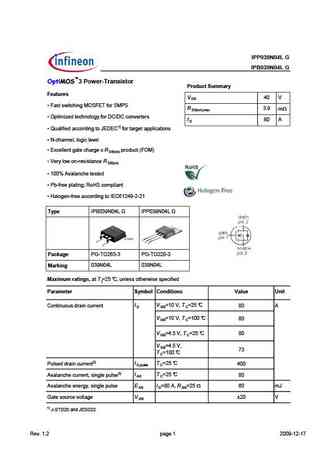
Type IPP039N04L G IPB039N04L G 3 Power-Transistor Product Summary Features V 40 V DS Fast switching MOSFET for SMPS R 3.9 mW DS(on),max Optimized technology for DC/DC converters I 80 A D Qualified according to JEDEC1) for target applications N-channel, logic level Excellent gate charge x R product (FOM) DS(on) Very low on-resistance R DS(on)
9.17. Size:1096K infineon
ipb032n10n5.pdf 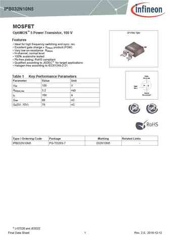
IPB032N10N5 MOSFET D -PAK 7pin OptiMOS 5 Power-Transistor, 100 V Features Ideal for high frequency switching and sync. rec. tab Excellent gate charge x R product (FOM) DS(on) Very low on-resistance R DS(on) N-channel, normal level 1 100% avalanche tested Pb-free plating; RoHS compliant 7 Qualified according to JEDEC1) for target applications H
9.18. Size:873K infineon
ipi041n12n3g ipp041n12n3g ipb038n12n3g.pdf 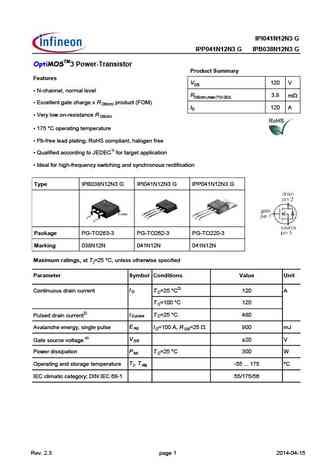
IPI041N12N3 G IPP041N12N3 G IPB038N12N3 G OptiMOSTM3 Power-Transistor Product Summary Features VDS 120 V N-channel, normal level RDS(on),max (TO-263) 3.8 mW Excellent gate charge x R product (FOM) DS(on) ID 120 A Very low on-resistance R DS(on) 175 C operating temperature Pb-free lead plating; RoHS compliant, halogen free Qualified according to JE
9.20. Size:723K infineon
ipb034n03l ipp034n03l.pdf 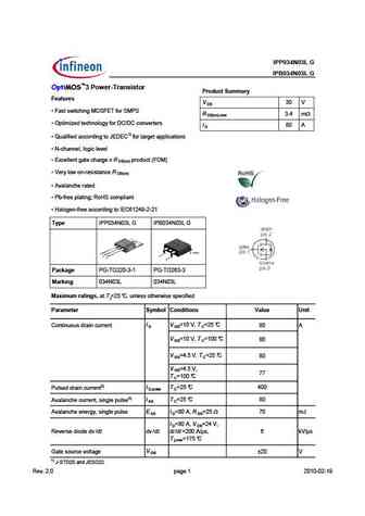
Type IPP034N03L G IPB034N03L G 3 Power-Transistor Product Summary Features V 30 V DS Fast switching MOSFET for SMPS R 3.4 mW DS(on),max Optimized technology for DC/DC converters I 80 A D Qualified according to JEDEC1) for target applications N-channel, logic level Excellent gate charge x R product (FOM) DS(on) Very low on-resistance R DS(on)
9.21. Size:258K inchange semiconductor
ipb033n10n5lf.pdf 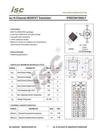
Isc N-Channel MOSFET Transistor IPB033N10N5LF FEATURES With To-263(D2PAK) package Low input capacitance and gate charge Low gate input resistance 100% avalanche tested Minimum Lot-to-Lot variations for robust device performance and reliable operation APPLICATIONS Switching applications ABSOLUTE MAXIMUM RATINGS(T =25 ) a SYMBOL PARAMETER VALUE UNIT V Drain-Source
9.22. Size:258K inchange semiconductor
ipb038n12n3g.pdf 
Isc N-Channel MOSFET Transistor IPB038N12N3G FEATURES With To-263(D2PAK) package Low input capacitance and gate charge Low gate input resistance 100% avalanche tested Minimum Lot-to-Lot variations for robust device performance and reliable operation APPLICATIONS Switching applications ABSOLUTE MAXIMUM RATINGS(T =25 ) a SYMBOL PARAMETER VALUE UNIT V Drain-Source
9.23. Size:243K inchange semiconductor
ipb034n03l .pdf 
isc N-Channel MOSFET Transistor IPB034N03L DESCRIPTION Drain Current I = 80A@ T =25 D C Drain Source Voltage V = 30V(Min) DSS 100% avalanche tested Minimum Lot-to-Lot variations for robust device performance and reliable operation APPLICATIONS . Designed for high current, high speed switching, switch mode power supplies. ABSOLUTE MAXIMUM RATINGS(T =25 ) C SY
9.24. Size:258K inchange semiconductor
ipb037n06n3.pdf 
Isc N-Channel MOSFET Transistor IPB037N06N3 FEATURES With To-263(D2PAK) package Low input capacitance and gate charge Low gate input resistance 100% avalanche tested Minimum Lot-to-Lot variations for robust device performance and reliable operation APPLICATIONS Switching applications ABSOLUTE MAXIMUM RATINGS(T =25 ) a SYMBOL PARAMETER VALUE UNIT V Drain-Source V
9.25. Size:258K inchange semiconductor
ipb034n06l3g.pdf 
Isc N-Channel MOSFET Transistor IPB034N06L3G FEATURES With To-263(D2PAK) package Low input capacitance and gate charge Low gate input resistance 100% avalanche tested Minimum Lot-to-Lot variations for robust device performance and reliable operation APPLICATIONS Switching applications ABSOLUTE MAXIMUM RATINGS(T =25 ) a SYMBOL PARAMETER VALUE UNIT V Drain-Source
9.26. Size:258K inchange semiconductor
ipb031n08n5.pdf 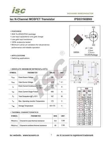
Isc N-Channel MOSFET Transistor IPB031N08N5 FEATURES With To-263(D2PAK) package Low input capacitance and gate charge Low gate input resistance 100% avalanche tested Minimum Lot-to-Lot variations for robust device performance and reliable operation APPLICATIONS Switching applications ABSOLUTE MAXIMUM RATINGS(T =25 ) a SYMBOL PARAMETER VALUE UNIT V Drain-Source V
9.27. Size:219K inchange semiconductor
ipb039n04l.pdf 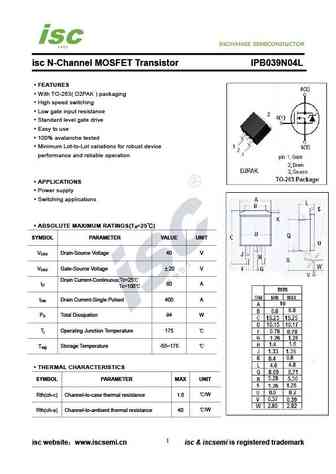
isc N-Channel MOSFET Transistor IPB039N04L FEATURES With TO-263( D2PAK ) packaging High speed switching Low gate input resistance Standard level gate drive Easy to use 100% avalanche tested Minimum Lot-to-Lot variations for robust device performance and reliable operation APPLICATIONS Power supply Switching applications ABSOLUTE MAXIMUM RATINGS(T =25 ) a
9.28. Size:243K inchange semiconductor
ipb034n03l.pdf 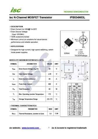
isc N-Channel MOSFET Transistor IPB034N03L DESCRIPTION Drain Current I = 80A@ T =25 D C Drain Source Voltage V = 30V(Min) DSS 100% avalanche tested Minimum Lot-to-Lot variations for robust device performance and reliable operation APPLICATIONS . Designed for high current, high speed switching, switch mode power supplies. ABSOLUTE MAXIMUM RATINGS(T =25 ) C SY
9.29. Size:252K inchange semiconductor
ipb031ne7n3.pdf 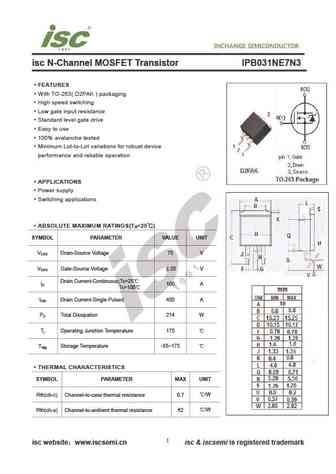
INCHANGE Semiconductor isc N-Channel MOSFET Transistor IPB031NE7N3 FEATURES With TO-263( D2PAK ) packaging High speed switching Low gate input resistance Standard level gate drive Easy to use 100% avalanche tested Minimum Lot-to-Lot variations for robust device performance and reliable operation APPLICATIONS Power supply Switching applications ABSOLUTE MAXI
Другие IGBT... IPB025N10N3G, IPB027N10N3G, IPB029N06N3G, IPB030N08N3G, IPB031NE7N3G, IPB034N03LG, IPB034N06L3G, IPB034N06N3G, 10N60, IPB036N12N3G, IPB037N06N3G, IPB038N12N3G, IPB039N04LG, IPB039N10N3G, IPB041N04NG, IPB042N03LG, IPB042N10N3G