APT6020LVR. Аналоги и основные параметры
Наименование производителя: APT6020LVR
Тип транзистора: MOSFET
Полярность: N
Предельные значения
Pd ⓘ
- Максимальная рассеиваемая мощность: 450 W
|Vds|ⓘ - Максимально допустимое напряжение сток-исток: 600 V
|Vgs|ⓘ - Максимально допустимое напряжение затвор-исток: 30 V
|Id| ⓘ - Максимально допустимый постоянный ток стока: 30 A
Tj ⓘ - Максимальная температура канала: 150 °C
Электрические характеристики
tr ⓘ -
Время нарастания: 12 ns
Cossⓘ - Выходная емкость: 650 pf
RDSonⓘ - Сопротивление сток-исток открытого транзистора: 0.2 Ohm
Тип корпуса: TO264
Аналог (замена) для APT6020LVR
- подборⓘ MOSFET транзистора по параметрам
APT6020LVR даташит
..1. Size:64K apt
apt6020lvr.pdf 
APT6020LVR 600V 30A 0.200 POWER MOS V Power MOS V is a new generation of high voltage N-Channel enhancement TO-264 mode power MOSFETs. This new technology minimizes the JFET effect, increases packing density and reduces the on-resistance. Power MOS V also achieves faster switching speeds through optimized gate layout.. Faster Switching 100% Avalanche Tested D Lower
8.1. Size:160K apt
apt6029bfllg apt6029sfllg.pdf 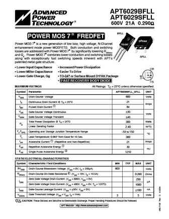
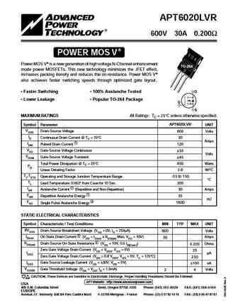
APT6029BFLL APT6029SFLL 600V 21A 0.290 BFLL R POWER MOS 7 FREDFET D3PAK Power MOS 7 is a new generation of low loss, high voltage, N-Channel TO-247 enhancement mode power MOSFETS. Both conduction and switching losses are addressed with Power MOS 7 by significantly lowering RDS(ON) and Qg. Power MOS 7 combines lower conduction and switching losses SFLL
8.2. Size:162K apt
apt6025bfllg apt6025sfllg.pdf 
APT6025BFLL APT6025SFLL 600V 24A 0.250 BFLL R POWER MOS 7 FREDFET D3PAK Power MOS 7 is a new generation of low loss, high voltage, N-Channel TO-247 enhancement mode power MOSFETS. Both conduction and switching losses are addressed with Power MOS 7 by significantly lowering RDS(ON) and Qg. Power MOS 7 combines lower conduction and switching losses SFLL
8.3. Size:69K apt
apt6025bll.pdf 
APT6025BLL APT6025SLL 600V 24A 0.250W TM BLL POWER MOS 7 Power MOS 7TM is a new generation of low loss, high voltage, N-Channel D3PAK TO-247 enhancement mode power MOSFETS. Both conduction and switching losses are addressed with Power MOS 7TM by significantly lowering RDS(ON) and Qg. Power MOS 7TM combines lower conduction and switching losses along with exceptionally fast switching
8.4. Size:116K apt
apt6025bvfrg apt6025svfrg.pdf 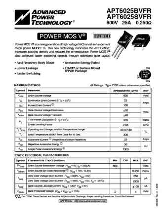
APT6025BVFR APT6025SVFR 600V 25A 0.250 POWER MOS V FREDFET D3PAK TO-247 Power MOS V is a new generation of high voltage N-Channel enhancement mode power MOSFETs. This new technology minimizes the JFET effect, increases packing density and reduces the on-resistance. Power MOS V also achieves faster switching speeds through optimized gate layout. Fast Re
8.5. Size:160K apt
apt6025bllg.pdf 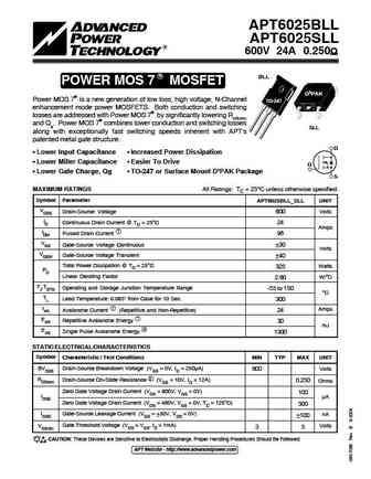
APT6025BLL APT6025SLL 600V 24A 0.250 R BLL POWER MOS 7 MOSFET D3PAK Power MOS 7 is a new generation of low loss, high voltage, N-Channel TO-247 enhancement mode power MOSFETS. Both conduction and switching losses are addressed with Power MOS 7 by significantly lowering RDS(ON) and Qg. Power MOS 7 combines lower conduction and switching losses SLL along
8.6. Size:49K apt
apt6025bvrg.pdf 
APT6025BVR 600V 25A 0.250 POWER MOS V Power MOS V is a new generation of high voltage N-Channel enhancement TO-247 mode power MOSFETs. This new technology minimizes the JFET effect, increases packing density and reduces the on-resistance. Power MOS V also achieves faster switching speeds through optimized gate layout. Faster Switching 100% Avalanche Tested D Lower L
8.7. Size:61K apt
apt6027hvr.pdf 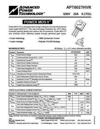
APT6027HVR 600V 20A 0.270 POWER MOS V TO-258 Power MOS V is a new generation of high voltage N-Channel enhancement mode power MOSFETs. This new technology minimizes the JFET effect, increases packing density and reduces the on-resistance. Power MOS V also achieves faster switching speeds through optimized gate layout. Faster Switching 100% Avalanche Tested D Lower
8.8. Size:113K apt
apt6025svfr.pdf 
APT6025BVFR APT6025SVFR 600V 25A 0.250 POWER MOS V FREDFET D3PAK TO-247 Power MOS V is a new generation of high voltage N-Channel enhancement mode power MOSFETs. This new technology minimizes the JFET effect, increases packing density and reduces the on-resistance. Power MOS V also achieves faster switching speeds through optimized gate layout. Fast Re
8.9. Size:72K apt
apt6025bvfr.pdf 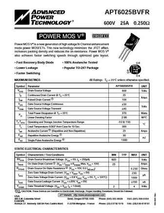
APT6025BVFR 600V 25A 0.250 POWER MOS V FREDFET Power MOS V is a new generation of high voltage N-Channel enhancement TO-247 mode power MOSFETs. This new technology minimizes the JFET effect, increases packing density and reduces the on-resistance. Power MOS V also achieves faster switching speeds through optimized gate layout. Fast Recovery Body Diode 100% Avalanche Test
8.10. Size:163K apt
apt6021bllg.pdf 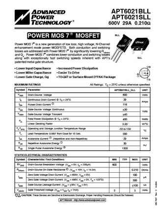
APT6021BLL APT6021SLL 600V 29A 0.210 R BLL POWER MOS 7 MOSFET D3PAK Power MOS 7 is a new generation of low loss, high voltage, N-Channel TO-247 enhancement mode power MOSFETS. Both conduction and switching losses are addressed with Power MOS 7 by significantly lowering RDS(ON) and Qg. Power MOS 7 combines lower conduction and switching losses SLL along
8.11. Size:71K apt
apt6029bfll.pdf 
APT6029BFLL APT6029SFLL 600V 21A 0.290W TM BFLL FREDFET POWER MOS 7 Power MOS 7TM is a new generation of low loss, high voltage, N-Channel D3PAK TO-247 enhancement mode power MOSFETS. Both conduction and switching losses are addressed with Power MOS 7TM by significantly lowering RDS(ON) and Qg. Power MOS 7TM combines lower conduction and switching losses along with exceptionally fas
8.12. Size:164K apt
apt6021bfllg apt6021sfllg.pdf 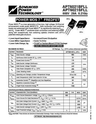
APT6021BFLL APT6021SFLL 600V 29A 0.210 R BFLL POWER MOS 7 FREDFET D3PAK Power MOS 7 is a new generation of low loss, high voltage, N-Channel TO-247 enhancement mode power MOSFETS. Both conduction and switching losses are addressed with Power MOS 7 by significantly lowering RDS(ON) and Qg. Power MOS 7 combines lower conduction and switching losses SFLL
8.13. Size:69K apt
apt6021bll.pdf 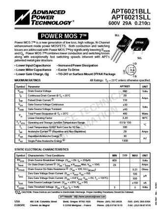
APT6021BLL APT6021SLL 600V 29A 0.210W TM BLL POWER MOS 7 Power MOS 7TM is a new generation of low loss, high voltage, N-Channel D3PAK TO-247 enhancement mode power MOSFETS. Both conduction and switching losses are addressed with Power MOS 7TM by significantly lowering RDS(ON) and Qg. Power MOS 7TM combines lower conduction and switching losses along with exceptionally fast switching
8.14. Size:160K apt
apt6029sll apt6029sllg.pdf 
APT6029BLL APT6029SLL 600V 21A 0.290 R BLL POWER MOS 7 MOSFET D3PAK Power MOS 7 is a new generation of low loss, high voltage, N-Channel TO-247 enhancement mode power MOSFETS. Both conduction and switching losses are addressed with Power MOS 7 by significantly lowering RDS(ON) and Qg. Power MOS 7 combines lower conduction and switching losses SLL along
8.15. Size:62K apt
apt6025bvr.pdf 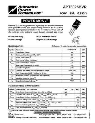
APT6025BVR 600V 25A 0.250 POWER MOS V Power MOS V is a new generation of high voltage N-Channel enhancement TO-247 mode power MOSFETs. This new technology minimizes the JFET effect, increases packing density and reduces the on-resistance. Power MOS V also achieves faster switching speeds through optimized gate layout. Faster Switching 100% Avalanche Tested D Lower L
8.16. Size:69K apt
apt6029bll.pdf 
APT6029BLL APT6029SLL 600V 21A 0.290W TM BLL POWER MOS 7 Power MOS 7TM is a new generation of low loss, high voltage, N-Channel D3PAK TO-247 enhancement mode power MOSFETS. Both conduction and switching losses are addressed with Power MOS 7TM by significantly lowering RDS(ON) and Qg. Power MOS 7TM combines lower conduction and switching losses along with exceptionally fast switching
8.17. Size:71K apt
apt6021bfll.pdf 
APT6021BFLL APT6021SFLL 600V 29A 0.210W TM BFLL FREDFET POWER MOS 7 Power MOS 7TM is a new generation of low loss, high voltage, N-Channel D3PAK TO-247 enhancement mode power MOSFETS. Both conduction and switching losses are addressed with Power MOS 7TM by significantly lowering RDS(ON) and Qg. Power MOS 7TM combines lower conduction and switching losses along with exceptionally fas
8.18. Size:71K apt
apt6025bfll.pdf 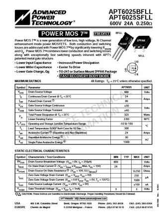
APT6025BFLL APT6025SFLL 600V 24A 0.250W TM BFLL FREDFET POWER MOS 7 Power MOS 7TM is a new generation of low loss, high voltage, N-Channel D3PAK TO-247 enhancement mode power MOSFETS. Both conduction and switching losses are addressed with Power MOS 7TM by significantly lowering RDS(ON) and Qg. Power MOS 7TM combines lower conduction and switching losses along with exceptionally fas
8.19. Size:59K apt
apt6025svr.pdf 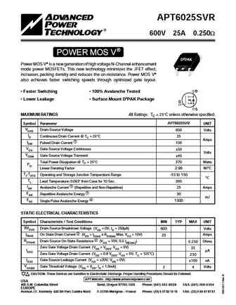
APT6025SVR 600V 25A 0.250W POWER MOS V D3PAK Power MOS V is a new generation of high voltage N-Channel enhancement mode power MOSFETs. This new technology minimizes the JFET effect, increases packing density and reduces the on-resistance. Power MOS V also achieves faster switching speeds through optimized gate layout. D Faster Switching 100% Avalanche Tested Lower Le
8.20. Size:376K inchange semiconductor
apt6025bll.pdf 
isc N-Channel MOSFET Transistor APT6025BLL FEATURES Drain Current I =24A@ T =25 D C Drain Source Voltage- V =600V(Min) DSS Static Drain-Source On-Resistance R =0.25 (Max) DS(on) 100% avalanche tested Minimum Lot-to-Lot variations for robust device performance and reliable operation DESCRIPTION Designed for use in switch mode power supplies and general purpo
8.21. Size:375K inchange semiconductor
apt6025bvfr.pdf 
isc N-Channel MOSFET Transistor APT6025BVFR FEATURES Drain Current I =25A@ T =25 D C Drain Source Voltage- V =600V(Min) DSS Static Drain-Source On-Resistance R =0.25 (Max) DS(on) 100% avalanche tested Minimum Lot-to-Lot variations for robust device performance and reliable operation DESCRIPTION Designed for use in switch mode power supplies and general purp
8.22. Size:376K inchange semiconductor
apt6029bfll.pdf 
isc N-Channel MOSFET Transistor APT6029BFLL FEATURES Drain Current I =21A@ T =25 D C Drain Source Voltage- V =600V(Min) DSS Static Drain-Source On-Resistance R =0.29 (Max) DS(on) 100% avalanche tested Minimum Lot-to-Lot variations for robust device performance and reliable operation DESCRIPTION Designed for use in switch mode power supplies and general purp
8.23. Size:376K inchange semiconductor
apt6021bll.pdf 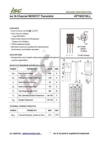
isc N-Channel MOSFET Transistor APT6021BLL FEATURES Drain Current I =29A@ T =25 D C Drain Source Voltage- V =600V(Min) DSS Static Drain-Source On-Resistance R =0.21 (Max) DS(on) 100% avalanche tested Minimum Lot-to-Lot variations for robust device performance and reliable operation DESCRIPTION Designed for use in switch mode power supplies and general purpo
8.24. Size:375K inchange semiconductor
apt6025bvr.pdf 
isc N-Channel MOSFET Transistor APT6025BVR FEATURES Drain Current I =25A@ T =25 D C Drain Source Voltage- V =600V(Min) DSS Static Drain-Source On-Resistance R =0.25 (Max) DS(on) 100% avalanche tested Minimum Lot-to-Lot variations for robust device performance and reliable operation DESCRIPTION Designed for use in switch mode power supplies and general purpo
8.25. Size:376K inchange semiconductor
apt6029bll.pdf 
isc N-Channel MOSFET Transistor APT6029BLL FEATURES Drain Current I =21A@ T =25 D C Drain Source Voltage- V =600V(Min) DSS Static Drain-Source On-Resistance R =0.29 (Max) DS(on) 100% avalanche tested Minimum Lot-to-Lot variations for robust device performance and reliable operation DESCRIPTION Designed for use in switch mode power supplies and general purpo
8.26. Size:376K inchange semiconductor
apt6021bfll.pdf 
isc N-Channel MOSFET Transistor APT6021BFLL FEATURES Drain Current I =29A@ T =25 D C Drain Source Voltage- V =600V(Min) DSS Static Drain-Source On-Resistance R =0.21 (Max) DS(on) 100% avalanche tested Minimum Lot-to-Lot variations for robust device performance and reliable operation DESCRIPTION Designed for use in switch mode power supplies and general purp
8.27. Size:376K inchange semiconductor
apt6025bfll.pdf 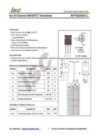
isc N-Channel MOSFET Transistor APT6025BFLL FEATURES Drain Current I =24A@ T =25 D C Drain Source Voltage- V =600V(Min) DSS Static Drain-Source On-Resistance R =0.25 (Max) DS(on) 100% avalanche tested Minimum Lot-to-Lot variations for robust device performance and reliable operation DESCRIPTION Designed for use in switch mode power supplies and general purp
Другие IGBT... APT50M85JVFR, APT50M85JVR, APT6013JVR, APT6015B2VR, APT6015JN, APT6015JVR, APT6015LVR, APT6017WVR, P60NF06, APT6025BVR, APT6027HVR, APT6030BN, APT6030BVR, APT6032AVR, APT6035AVR, APT6035BN, APT6035BVR
