Справочник MOSFET. IPP111N15N3G


IPP111N15N3G MOSFET - описание производителя. Даташиты. Основные параметры и характеристики. Поиск аналога. Справочник


   Наименование прибора: IPP111N15N3G
   Маркировка: 111N15N
   Тип транзистора: MOSFET
   Полярность: N
   Максимальная рассеиваемая мощность (Pd): 214 W
   Предельно допустимое напряжение сток-исток |Uds|: 150 V
   Предельно допустимое напряжение затвор-исток |Ugs|: 20 V
   Пороговое напряжение включения |Ugs(th)|: 4 V
   Максимально допустимый постоянный ток стока |Id|: 83 A
   Максимальная температура канала (Tj): 175 °C
   Общий заряд затвора (Qg): 41 nC
   Время нарастания (tr): 35 ns
   Выходная емкость (Cd): 378 pf
   Сопротивление сток-исток открытого транзистора (Rds): 0.0111 Ohm
   Тип корпуса: TO220

 Аналог (замена) для IPP111N15N3G


IPP111N15N3G Datasheet (PDF)

 ..1. Size:757K  infineon
ipb108n15n3g ipp111n15n3g ipi111n15n3g.pdf
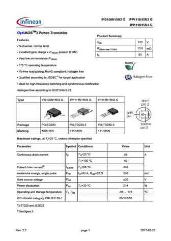
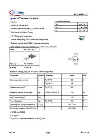
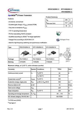
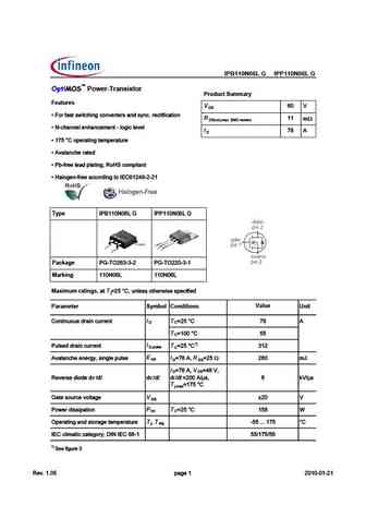
IPP111N15N3G
IPP111N15N3G

IPB108N15N3 G IPP111N15N3 GIPI111N15N3 GOptiMOSTM3 Power-TransistorProduct Summary FeaturesVDS 150 V N-channel, normal levelRDS(on),max (TO263) 10.8 mW Excellent gate charge x R product (FOM)DS(on)ID 83 A Very low on-resistance RDS(on) 175 C operating temperature Pb-free lead plating; RoHS compliant; Halogen free Qualified according to JEDE

 3.1. Size:438K  infineon
ipb108n15n3-g ipp111n15n3-g ipi111n15n3-g.pdf
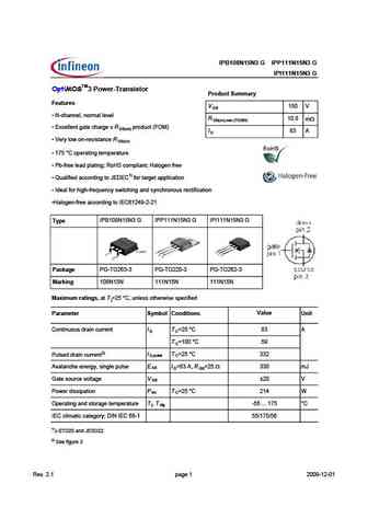
IPP111N15N3G
IPP111N15N3G

IPB108N15N3 G IPP111N15N3 GIPI111N15N3 GOptiMOSTM3 Power-TransistorProduct SummaryFeaturesV 150 VDS N-channel, normal levelR 10.8mDS(on),max (TO263) Excellent gate charge x R product (FOM)DS(on)I 83 AD Very low on-resistance RDS(on) 175 C operating temperature Pb-free lead plating; RoHS compliant; Halogen free Qualified according to JE

 3.2. Size:245K  inchange semiconductor
ipp111n15n3.pdf

IPP111N15N3G
IPP111N15N3G

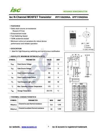
isc N-Channel MOSFET Transistor IPP111N15N3IIPP111N15N3FEATURESStatic drain-source on-resistance:RDS(on) 11.1mEnhancement modeFast Switching Speed100% avalanche testedMinimum Lot-to-Lot variations for robust deviceperformance and reliable operationDESCRITIONIdeal for high-frequency switching and synchronous rectificationABSOLUTE MAXIMUM RATINGS(T

 9.1. Size:300K  infineon
ipb114n03l-g ipp114n03l-g.pdf
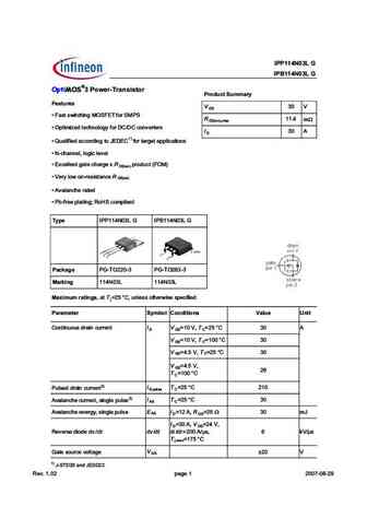
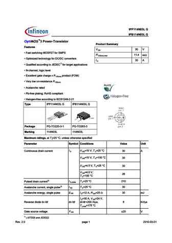
IPP111N15N3G
IPP111N15N3G

Type IPP114N03L GIPB114N03L GOptiMOS3 Power-TransistorProduct SummaryFeaturesV 30 VDS Fast switching MOSFET for SMPSR 11.4mDS(on),max Optimized technology for DC/DC convertersI 30 AD Qualified according to JEDEC1) for target applications N-channel, logic level Excellent gate charge x R product (FOM)DS(on) Very low on-resistance RDS(on

 9.2. Size:652K  infineon
ipb107n20na ipp110n20na.pdf

IPP111N15N3G
IPP111N15N3G

IPB107N20NA IPP110N20NAOptiMOSTM3 Power-TransistorProduct SummaryFeaturesVDS 200 V N-channel, normal levelRDS(on),max (TO263) 10.7mW Excellent gate charge x R product (FOM)DS(on)ID 88 A Very low on-resistance RDS(on) 175 C operating temperature Pb-free lead plating; RoHS compliant Qualified according to AEC Q101 Halogen-free according to IE

 9.3. Size:304K  infineon
ipp114n12n3g.pdf

IPP111N15N3G
IPP111N15N3G

IPP114N12N3 GOptiMOSTM3 Power-TransistorProduct SummaryFeaturesVDS 120 V N-channel, normal levelRDS(on)max 11.4m Excellent gate charge x R product (FOM)DS(on)ID 75 A Very low on-resistance RDS(on) 175 C operating temperature Pb-free lead plating; RoHS compliant; halogen free Qualified according to JEDEC1) for target application Ideal for

 9.4. Size:690K  infineon
ipb107n20n3-g ipp110n20n3-g ipi110n20n3-g ipb107n20n3g ipp110n20n3g ipi110n20n3g.pdf

IPP111N15N3G
IPP111N15N3G

IPB107N20N3 G IPP110N20N3 GIPI110N20N3 GOptiMOSTM3 Power-TransistorProduct SummaryFeaturesVDS 200 V N-channel, normal levelRDS(on),max (TO263) 10.7mW Excellent gate charge x R product (FOM)DS(on)ID 88 A Very low on-resistance RDS(on) 175 C operating temperature Pb-free lead plating; RoHS compliant Qualified according to JEDEC1) for target appl

 9.5. Size:617K  infineon
ipp114n03l.pdf

IPP111N15N3G
IPP111N15N3G

pe %% # ! % # ! % (>.;?6?@%>EFeaturesD Q 2CD CG:D49:?8 ') - . 7@B -'*- 11 4m - @? >2H Q ) AD:>:J65 D649?@=@8I 7@B 4@?F6BD6BCD1)Q + E2=:7:65 244@B5:?8 D@ $ 7@B D2B86D 2AA=:42D:@?CQ ( 492??6= =@8:4 =6F6=Q H46==6?D 82D6 492B86 H AB@5E4D ) ' D n)Q /6BI =@G @? B6C:CD2?46 D n)Q F2=2?496 B2D65Q *3 7B66 A=2D:?8 , @"- 4@>A=:2?DQ "2=@86? 7B6

 9.6. Size:740K  infineon
ipb110n06lg ipp110n06lg.pdf

IPP111N15N3G
IPP111N15N3G

IPB110N06L G IPP110N06L G Power-TransistorProduct SummaryFeaturesV D P ?A 61BC BF9C389>7 3?>E5AC5AB 1>4 BH>3 A53C96931C9?>R 11 m , ?> =1G ,' E5AB9?>P ( 381>>581>35=5>C

 9.7. Size:245K  inchange semiconductor
ipp114n12n3.pdf

IPP111N15N3G
IPP111N15N3G

isc N-Channel MOSFET Transistor IPP114N12N3IIPP114N12N3FEATURESStatic drain-source on-resistance:RDS(on) 11.4mEnhancement modeFast Switching Speed100% avalanche testedMinimum Lot-to-Lot variations for robust deviceperformance and reliable operationDESCRITION Ideal for high-frequency switching and synchronous rectificationABSOLUTE MAXIMUM RATINGS(

 9.8. Size:245K  inchange semiconductor
ipp110n20n3.pdf

IPP111N15N3G
IPP111N15N3G

isc N-Channel MOSFET Transistor IPP110N20N3IIPP110N20N3FEATURESStatic drain-source on-resistance:RDS(on) 11mEnhancement modeFast Switching Speed100% avalanche testedMinimum Lot-to-Lot variations for robust deviceperformance and reliable operationDESCRITIONIdeal for high-frequency switching and synchronous rectificationABSOLUTE MAXIMUM RATINGS(T =

 9.9. Size:245K  inchange semiconductor
ipp110n20na.pdf

IPP111N15N3G
IPP111N15N3G

isc N-Channel MOSFET Transistor IPP110N20NAIIPP110N20NAFEATURESStatic drain-source on-resistance:RDS(on) 11mEnhancement modeFast Switching Speed100% avalanche testedMinimum Lot-to-Lot variations for robust deviceperformance and reliable operationDESCRITION Ideal for high-frequency switching and synchronous rectificationABSOLUTE MAXIMUM RATINGS(T

Другие MOSFET... IRFP360LC , IRFP3710 , IRFP430 , IRFP431 , IRFP432 , IRFP433 , IRFP440 , IRFP440A , MMIS60R580P , IRFP442 , IRFP443 , IRFP448 , IRFP450 , IRFP450A , IRFP450FI , IRFP450LC , IRFP451 .


Back to Top