Аналоги IRFS5615. Основные параметры
Наименование производителя: IRFS5615
Тип транзистора: MOSFET
Полярность: N
Pd ⓘ - Максимальная рассеиваемая мощность: 144
W
|Vds|ⓘ - Предельно допустимое напряжение сток-исток: 150
V
|Vgs|ⓘ - Предельно допустимое напряжение затвор-исток: 20
V
|Id| ⓘ - Максимально
допустимый постоянный ток стока: 33
A
Tj ⓘ - Максимальная температура канала: 175
°C
tr ⓘ -
Время нарастания: 23.1
ns
Cossⓘ - Выходная емкость: 155
pf
Rds ⓘ - Сопротивление сток-исток открытого транзистора: 0.042
Ohm
Тип корпуса:
D2PAK
Аналог (замена) для IRFS5615
-
подбор ⓘ MOSFET транзистора по параметрам
IRFS5615 даташит
..1. Size:345K international rectifier
irfs5615pbf irfsl5615pbf.pdf 
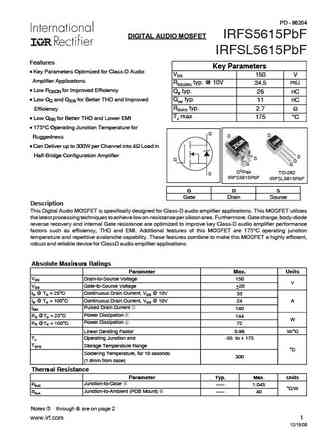
PD - 96204 DIGITAL AUDIO MOSFET IRFS5615PbF IRFSL5615PbF Features Key Parameters Key Parameters Optimized for Class-D Audio VDS 150 V Amplifier Applications RDS(ON) typ. @ 10V m 34.5 Low RDSON for Improved Efficiency Qg typ. 26 nC Low QG and QSW for Better THD and Improved Qsw typ. 11 nC RG(int) typ. Efficiency 2.7 TJ max 175 C Low QRR for Better THD
..2. Size:257K inchange semiconductor
irfs5615.pdf 
Isc N-Channel MOSFET Transistor IRFS5615 FEATURES With To-263(D2PAK) package Low input capacitance and gate charge Low gate input resistance 100% avalanche tested Minimum Lot-to-Lot variations for robust device performance and reliable operation APPLICATIONS Switching applications ABSOLUTE MAXIMUM RATINGS(T =25 ) a SYMBOL PARAMETER VALUE UNIT V Drain-Source Volt
8.1. Size:333K international rectifier
irfs5620pbf irfsl5620pbf.pdf 
PD - 96205 DIGITAL AUDIO MOSFET IRFS5620PbF Features IRFSL5620PbF Key Parameters Optimized for Class-D Audio Key Parameters Amplifier Applications VDS 200 V Low RDSON for Improved Efficiency RDS(ON) typ. @ 10V m 63.7 Low QG and QSW for Better THD and Improved Qg typ. 25 nC Efficiency Qsw typ. 9.8 nC Low QRR for Better THD and Lower EMI RG(int) typ. 2.6
9.2. Size:257K 1
irfs510a.pdf 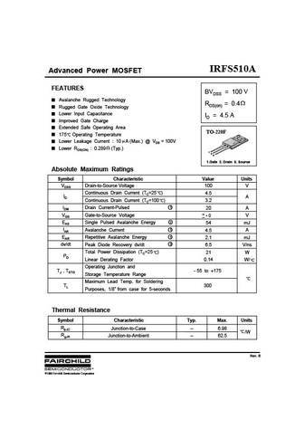
IRFS510A Advanced Power MOSFET FEATURES BVDSS = 100 V Avalanche Rugged Technology RDS(on) = 0.4 Rugged Gate Oxide Technology Lower Input Capacitance ID = 4.5 A Improved Gate Charge Extended Safe Operating Area TO-220F 175 C Operating Temperature Lower Leakage Current 10 A (Max.) @ VDS = 100V Lower RDS(ON) 0.289 (Typ.) 1 2 3 1.Gate 2. Drain 3. So
9.4. Size:325K international rectifier
irfb52n15dpbf irfs52n15dpbf.pdf 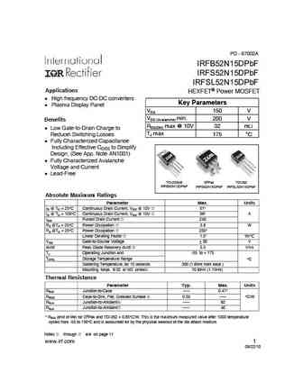
PD - 97002A IRFB52N15DPbF IRFS52N15DPbF IRFSL52N15DPbF Applications HEXFET Power MOSFET l High frequency DC-DC converters Key Parameters l Plasma Display Panel VDS 150 V VDS (Avalanche) min. 200 V Benefits RDS(ON) max @ 10V 32 m l Low Gate-to-Drain Charge to TJ max Reduce Switching Losses 175 C l Fully Characterized Capacitance Including Effective COSS to Simplify Design
9.5. Size:325K international rectifier
irfb52n15dpbf irfs52n15dpbf irfsl52n15dpbf.pdf 
PD - 97002A IRFB52N15DPbF IRFS52N15DPbF IRFSL52N15DPbF Applications HEXFET Power MOSFET l High frequency DC-DC converters Key Parameters l Plasma Display Panel VDS 150 V VDS (Avalanche) min. 200 V Benefits RDS(ON) max @ 10V 32 m l Low Gate-to-Drain Charge to TJ max Reduce Switching Losses 175 C l Fully Characterized Capacitance Including Effective COSS to Simplify Design
9.6. Size:227K international rectifier
irfb59n10dpbf irfs59n10dpbf.pdf 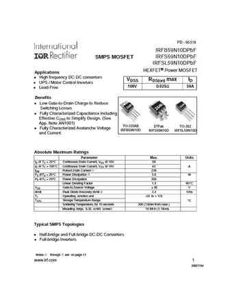
PD - 95378 IRFB59N10DPbF IRFS59N10DPbF SMPS MOSFET IRFSL59N10DPbF HEXFET Power MOSFET Applications l High frequency DC-DC converters VDSS RDS(on) max ID l UPS / Motor Control Inverters 100V 0.025 59A l Lead-Free Benefits l Low Gate-to-Drain Charge to Reduce Switching Losses l Fully Characterized Capacitance Including Effective COSS to Simplify Design, (See App. Note AN1
9.7. Size:138K international rectifier
irfs59n10d.pdf 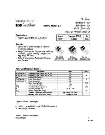
PD - 93890 IRFB59N10D IRFS59N10D SMPS MOSFET IRFSL59N10D HEXFET Power MOSFET Applications VDSS RDS(on) max ID High frequency DC-DC converters 100V 0.025 59A Benefits Low Gate-to-Drain Charge to Reduce Switching Losses Fully Characterized Capacitance Including Effective COSS to Simplify Design, (See App. Note AN1001) TO-220AB D2Pak TO-262 Fully Characterized Avalanc
9.8. Size:134K international rectifier
irfs52n15d.pdf 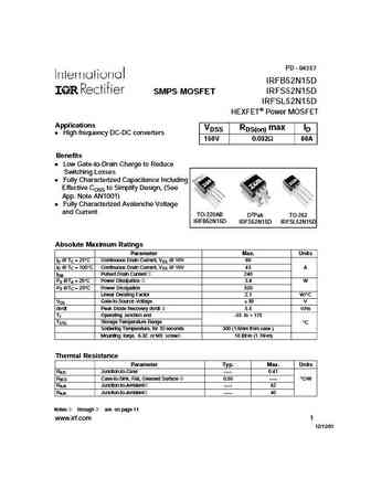
PD - 94357 IRFB52N15D IRFS52N15D SMPS MOSFET IRFSL52N15D HEXFET Power MOSFET Applications VDSS RDS(on) max ID High frequency DC-DC converters 150V 0.032 60A Benefits Low Gate-to-Drain Charge to Reduce Switching Losses Fully Characterized Capacitance Including Effective COSS to Simplify Design, (See App. Note AN1001) Fully Characterized Avalanche Voltage and Current
9.9. Size:227K international rectifier
irfb59n10dpbf irfs59n10dpbf irfsl59n10dpbf.pdf 
PD - 95378 IRFB59N10DPbF IRFS59N10DPbF SMPS MOSFET IRFSL59N10DPbF HEXFET Power MOSFET Applications l High frequency DC-DC converters VDSS RDS(on) max ID l UPS / Motor Control Inverters 100V 0.025 59A l Lead-Free Benefits l Low Gate-to-Drain Charge to Reduce Switching Losses l Fully Characterized Capacitance Including Effective COSS to Simplify Design, (See App. Note AN1
9.10. Size:504K samsung
irfs520a.pdf 
Advanced Power MOSFET FEATURES BVDSS = 100 V Avalanche Rugged Technology RDS(on) = 0.2 Rugged Gate Oxide Technology Lower Input Capacitance ID = 7.2 A Improved Gate Charge Extended Safe Operating Area 175 Operating Temperature Lower Leakage Current 10 A (Max.) @ VDS = 100V Lower RDS(ON) 0.155 (Typ.) 1 2 3 1.Gate 2. Drain 3. Source Absolute Maximu
9.12. Size:509K samsung
irfs530a.pdf 
Advanced Power MOSFET FEATURES BVDSS = 100 V Avalanche Rugged Technology RDS(on) = 0.11 Rugged Gate Oxide Technology Lower Input Capacitance ID = 10.7 A Improved Gate Charge Extended Safe Operating Area 175 Operating Temperature Lower Leakage Current 10 A (Max.) @ VDS = 100V Lower RDS(ON) 0.092 (Typ.) 1 2 3 1.Gate 2. Drain 3. Source Absolute Maxim
9.13. Size:510K samsung
irfs550a.pdf 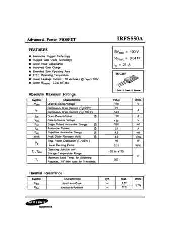
Advanced Power MOSFET FEATURES BVDSS = 100 V Avalanche Rugged Technology RDS(on) = 0.04 Rugged Gate Oxide Technology Lower Input Capacitance ID = 21 A Improved Gate Charge Extended Safe Operating Area 175 Operating Temperature Lower Leakage Current 10 A (Max.) @ VDS = 100V Lower RDS(ON) 0.032 (Typ.) 1 2 3 1.Gate 2. Drain 3. Source Absolute Maximum
9.14. Size:507K samsung
irfs540a.pdf 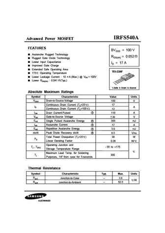
Advanced Power MOSFET FEATURES BVDSS = 100 V Avalanche Rugged Technology RDS(on) = 0.052 Rugged Gate Oxide Technology Lower Input Capacitance ID = 17 A Improved Gate Charge Extended Safe Operating Area 175 Operating Temperature Lower Leakage Current 10 A (Max.) @ VDS = 100V Lower RDS(ON) 0.041 (Typ.) 1 2 3 1.Gate 2. Drain 3. Source Absolute Maximum
9.16. Size:257K inchange semiconductor
irfs59n10d.pdf 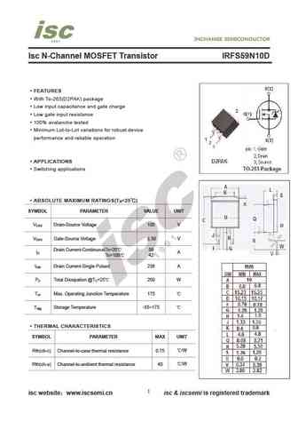
Isc N-Channel MOSFET Transistor IRFS59N10D FEATURES With To-263(D2PAK) package Low input capacitance and gate charge Low gate input resistance 100% avalanche tested Minimum Lot-to-Lot variations for robust device performance and reliable operation APPLICATIONS Switching applications ABSOLUTE MAXIMUM RATINGS(T =25 ) a SYMBOL PARAMETER VALUE UNIT V Drain-Source Vo
9.17. Size:241K inchange semiconductor
irfs52n15d.pdf 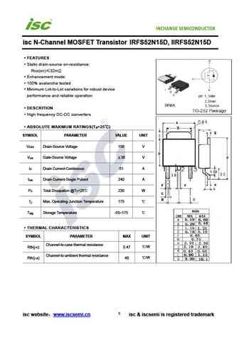
isc N-Channel MOSFET Transistor IRFS52N15D, IIRFS52N15D FEATURES Static drain-source on-resistance RDS(on) 32m Enhancement mode 100% avalanche tested Minimum Lot-to-Lot variations for robust device performance and reliable operation DESCRITION High frequency DC-DC converters ABSOLUTE MAXIMUM RATINGS(T =25 ) a SYMBOL PARAMETER VALUE UNIT V Drain-Source Volta
Другие MOSFET... IRFS4310Z
, IRFS4321
, IRFS4410
, IRFS4410Z
, IRFS4610
, IRFS4615
, IRFS4620
, IRFS52N15D
, IRFZ44N
, IRFS5620
, IRFS59N10D
, IRFSL23N20D
, IRFSL3004
, IRFSL3006
, IRFSL3107
, IRFSL31N20D
, IRFSL3206
.