CEP04N6. Аналоги и основные параметры
Наименование производителя: CEP04N6
Тип транзистора: MOSFET
Полярность: N
Предельные значения
Pd ⓘ
- Максимальная рассеиваемая мощность: 104 W
|Vds|ⓘ - Максимально допустимое напряжение сток-исток: 600 V
|Vgs|ⓘ - Максимально допустимое напряжение затвор-исток: 30 V
|Id| ⓘ - Максимально допустимый постоянный ток стока: 4.2 A
Tj ⓘ - Максимальная температура канала: 150 °C
Электрические характеристики
tr ⓘ -
Время нарастания: 18 ns
Cossⓘ - Выходная емкость: 75 pf
RDSonⓘ - Сопротивление сток-исток открытого транзистора: 2.4 Ohm
Тип корпуса: TO220
Аналог (замена) для CEP04N6
- подборⓘ MOSFET транзистора по параметрам
CEP04N6 даташит
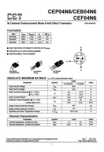
..1. Size:357K cet
cep04n6 ceb04n6 cef04n6.pdf 

CEP04N6/CEB04N6 CEF04N6 PRELIMINARY N-Channel Enhancement Mode Field Effect Transistor FEATURES Type VDSS RDS(ON) ID @VGS CEP04N6 600V 2.4 4.2A 10V CEB04N6 600V 2.4 4.2A 10V CEF04N6 600V 2.4 4.2A d 10V D Super high dense cell design for extremely low RDS(ON). High power and current handing capability. Lead-free plating ; RoHS compliant. G S CEB SERIES CEP SERIES CEF SER
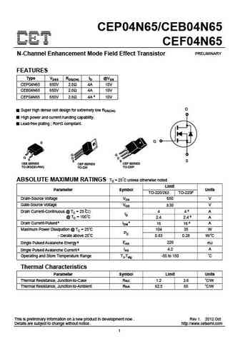
0.1. Size:358K cet
cep04n65 ceb04n65 cef04n65.pdf 

CEP04N65/CEB04N65 CEF04N65 PRELIMINARY N-Channel Enhancement Mode Field Effect Transistor FEATURES Type VDSS RDS(ON) ID @VGS CEP04N65 650V 2.8 4A 10V CEB04N65 650V 2.8 4A 10V CEF04N65 650V 2.8 4A d 10V D Super high dense cell design for extremely low RDS(ON). High power and current handing capability. Lead-free plating ; RoHS compliant. G S CEB SERIES CEP SERIES CEF SER
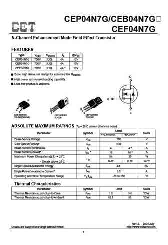
8.1. Size:440K cet
cep04n7g ceb04n7g cef04n7g.pdf 

CEP04N7G/CEB04N7G CEF04N7G N-Channel Enhancement Mode Field Effect Transistor FEATURES Type VDSS RDS(ON) ID @VGS CEP04N7G 700V 3.3 4A 10V CEB04N7G 700V 3.3 4A 10V CEF04N7G 700V 3.3 4A d 10V Super high dense cell design for extremely low RDS(ON). D High power and current handing capability. Lead free product is acquired. G S CEB SERIES CEP SERIES CEF SERIES TO-263(DD-PA
9.1. Size:400K ncepower
ncep040n12d.pdf 

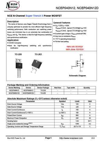
NCEP040N12, NCEP040N12D NCE N-Channel Super Trench II Power MOSFET Description General Features The series of devices uses Super Trench II technology that is VDS =120V,ID =150A uniquely optimized to provide the most efficient high frequency RDS(ON)=3.5m , typical (TO-220)@ VGS=10V switching performance. Both conduction and switching power RDS(ON)=3.3m , typical (TO-2
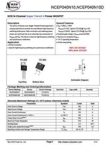
9.2. Size:363K ncepower
ncep040n10.pdf 

NCEP040N10,NCEP040N10D NCE N-Channel Super Trench II Power MOSFET Description General Features The series of devices uses Super Trench II technology that is VDS =100V,ID =130A uniquely optimized to provide the most efficient high frequency RDS(ON)=3.7m , typical (TO-220)@ VGS=10V switching performance. Both conduction and switching power RDS(ON)=3.55m , typical (TO-263)@ VGS=
9.3. Size:363K ncepower
ncep040n10d.pdf 

NCEP040N10,NCEP040N10D NCE N-Channel Super Trench II Power MOSFET Description General Features The series of devices uses Super Trench II technology that is VDS =100V,ID =130A uniquely optimized to provide the most efficient high frequency RDS(ON)=3.7m , typical (TO-220)@ VGS=10V switching performance. Both conduction and switching power RDS(ON)=3.55m , typical (TO-263)@ VGS=
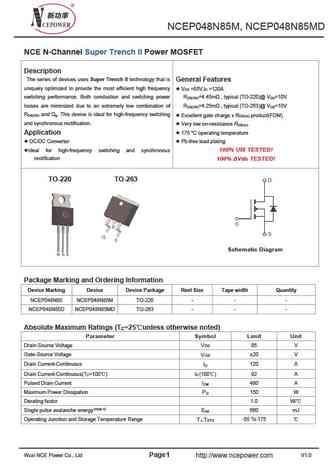
9.4. Size:761K ncepower
ncep048n85md.pdf 

NCEP048N85M, NCEP048N85MD NCE N-Channel Super Trench II Power MOSFET Description The series of devices uses Super Trench II technology that is General Features uniquely optimized to provide the most efficient high frequency V =85V,I =120A DS D switching performance. Both conduction and switching power R =4.45m , typical (TO-220)@ V =10V DS(ON) GS losses are minimized due to an e
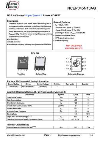
9.5. Size:323K ncepower
ncep045n10ag.pdf 

NCEP045N10AG NCE N-Channel Super Trench II Power MOSFET Description General Features The series of devices uses Super Trench II technology that is VDS =100V,ID =125A uniquely optimized to provide the most efficient high frequency RDS(ON)=4.0m , typical @ VGS=10V switching performance. Both conduction and switching power RDS(ON)=5.0m , typical @ VGS=4.5V losses are m
9.6. Size:371K ncepower
ncep045n10 ncep045n10d.pdf 

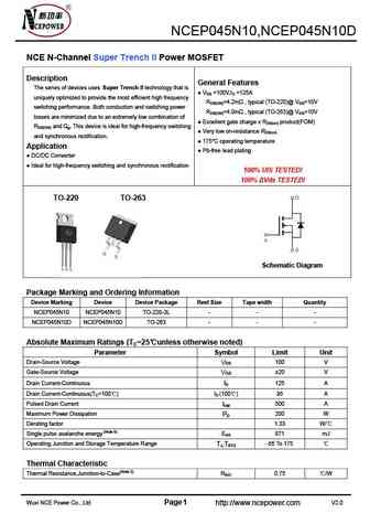
NCEP045N10,NCEP045N10D NCE N-Channel Super Trench II Power MOSFET Description General Features The series of devices uses Super Trench II technology that is VDS =100V,ID =125A uniquely optimized to provide the most efficient high frequency RDS(ON)=4.2m , typical (TO-220)@ VGS=10V switching performance. Both conduction and switching power RDS(ON)=4.0m , typical (TO-263
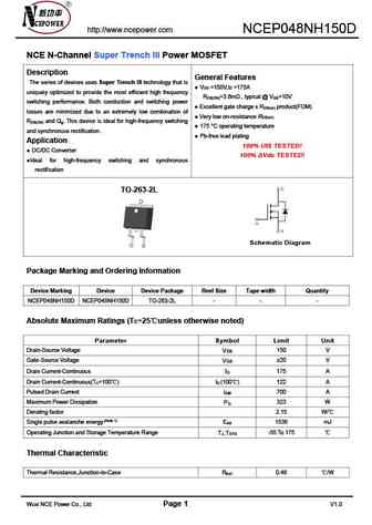
9.7. Size:789K ncepower
ncep048nh150d.pdf 

http //www.ncepower.com NCEP048NH150D NCE N-Channel Super Trench III Power MOSFET Description General Features The series of devices uses Super Trench III technology that is V =150V,I =175A DS D uniquely optimized to provide the most efficient high frequency R =3.6m , typical @ V =10V DS(ON) GS switching performance. Both conduction and switching power Excellent gate charge
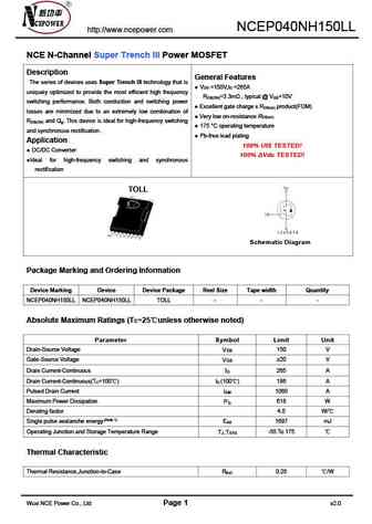
9.8. Size:756K ncepower
ncep040nh150ll.pdf 

NCEP040NH150LL http //www.ncepower.com NCE N-Channel Super Trench III Power MOSFET Description General Features The series of devices uses Super Trench III technology that is V =150V,I =265A DS D uniquely optimized to provide the most efficient high frequency R =3.3m , typical @ V =10V DS(ON) GS switching performance. Both conduction and switching power Excellent gate char
9.9. Size:699K ncepower
ncep040n85.pdf 

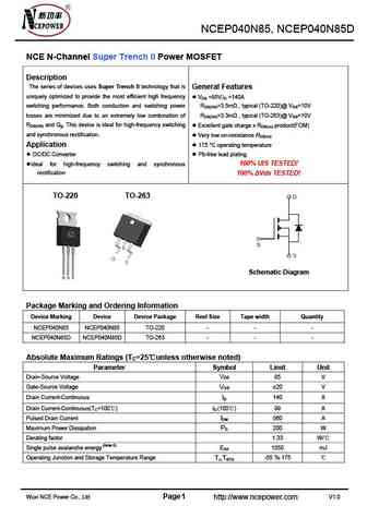
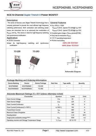
NCEP040N85, NCEP040N85D NCE N-Channel Super Trench II Power MOSFET Description The series of devices uses Super Trench II technology that is General Features uniquely optimized to provide the most efficient high frequency V =85V,I =140A DS D switching performance. Both conduction and switching power R =3.5m , typical (TO-220)@ V =10V DS(ON) GS losses are minimized due to an extr
9.10. Size:1002K ncepower
ncep040n85m.pdf 

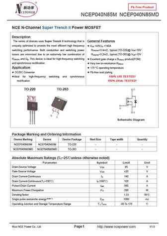
Pb Free Product NCEP040N85M NCEP040N85MD NCE N-Channel Super Trench II Power MOSFET Description The series of devices uses Super Trench II technology that is General Features uniquely optimized to provide the most efficient high frequency V =85V,I =140A DS D switching performance. Both conduction and switching power R =3.4m , typical (TO-220)@ V =10V DS(ON) GS losses are minimi
9.11. Size:835K ncepower
ncep048n85 ncep048n85d.pdf 

NCEP048N85M, NCEP048N85MD NCE N-Channel Super Trench II Power MOSFET Description The series of devices uses Super Trench II technology that is General Features uniquely optimized to provide the most efficient high frequency V =85V,I =120A DS D switching performance. Both conduction and switching power R =4.45m , typical (TO-220)@ V =10V DS(ON) GS losses are minimized due to an e
9.12. Size:371K ncepower
ncep045n10d.pdf 

NCEP045N10,NCEP045N10D NCE N-Channel Super Trench II Power MOSFET Description General Features The series of devices uses Super Trench II technology that is VDS =100V,ID =125A uniquely optimized to provide the most efficient high frequency RDS(ON)=4.2m , typical (TO-220)@ VGS=10V switching performance. Both conduction and switching power RDS(ON)=4.0m , typical (TO-263
9.13. Size:354K ncepower
ncep045n10g.pdf 

http //www.ncepower.com NCEP045N10G NCE N-Channel Super Trench II Power MOSFET Description General Features The NCEP045N10G uses Super Trench II technology that is VDS =100V,ID =125A uniquely optimized to provide the most efficient high frequency RDS(ON)=3.8m (typical) @ VGS=10V switching performance. Both conduction and switching power Excellent gate charge x RDS(on
9.14. Size:835K ncepower
ncep048n85.pdf 

NCEP048N85M, NCEP048N85MD NCE N-Channel Super Trench II Power MOSFET Description The series of devices uses Super Trench II technology that is General Features uniquely optimized to provide the most efficient high frequency V =85V,I =120A DS D switching performance. Both conduction and switching power R =4.45m , typical (TO-220)@ V =10V DS(ON) GS losses are minimized due to an e
9.15. Size:1002K ncepower
ncep040n85md.pdf 

Pb Free Product NCEP040N85M NCEP040N85MD NCE N-Channel Super Trench II Power MOSFET Description The series of devices uses Super Trench II technology that is General Features uniquely optimized to provide the most efficient high frequency V =85V,I =140A DS D switching performance. Both conduction and switching power R =3.4m , typical (TO-220)@ V =10V DS(ON) GS losses are minimi
9.16. Size:673K ncepower
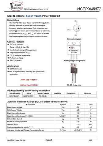
ncep048n72.pdf 

http //www.ncepower.com NCEP048N72 NCE N-Channel Super Trench Power MOSFET Description The NCEP048N72 uses Super Trench technology that is uniquely optimized to provide the most efficient high frequency switching performance. Both conduction and switching power losses are minimized due to an extremely low combination of R and Q . This device is ideal for DS(ON) g high-frequency switch
9.17. Size:323K ncepower
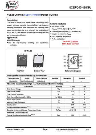
ncep045n85gu.pdf 

NCEP045N85GU NCE N-Channel Super Trench II Power MOSFET Description The series of devices uses Super Trench II technology that is General Features uniquely optimized to provide the most efficient high frequency VDS =85V,ID =110A switching performance. Both conduction and switching power RDS(ON)=4.1m , typical @ VGS=10V losses are minimized due to an extremely low combin
9.18. Size:761K ncepower
ncep048n85m ncep048n85md.pdf 

NCEP048N85M, NCEP048N85MD NCE N-Channel Super Trench II Power MOSFET Description The series of devices uses Super Trench II technology that is General Features uniquely optimized to provide the most efficient high frequency V =85V,I =120A DS D switching performance. Both conduction and switching power R =4.45m , typical (TO-220)@ V =10V DS(ON) GS losses are minimized due to an e
9.19. Size:761K ncepower
ncep048n85m.pdf 

NCEP048N85M, NCEP048N85MD NCE N-Channel Super Trench II Power MOSFET Description The series of devices uses Super Trench II technology that is General Features uniquely optimized to provide the most efficient high frequency V =85V,I =120A DS D switching performance. Both conduction and switching power R =4.45m , typical (TO-220)@ V =10V DS(ON) GS losses are minimized due to an e
9.20. Size:1123K ncepower
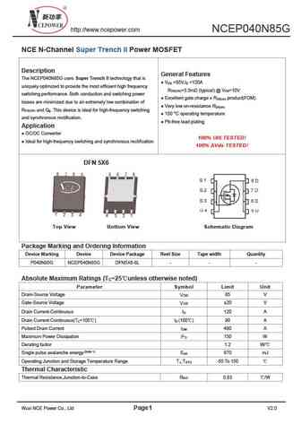
ncep040n85g.pdf 

http //www.ncepower.com NCEP040N85G NCE N-Channel Super Trench II Power MOSFET Description General Features The NCEP040N85G uses Super Trench II technology that is V =85V,I =120A DS D uniquely optimized to provide the most efficient high frequency R =3.5m (typical) @ V =10V DS(ON) GS switching performance. Both conduction and switching power Excellent gate charge x R produc
9.21. Size:683K ncepower
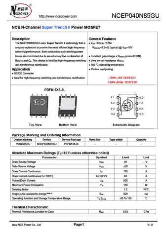
ncep040n85gu.pdf 

http //www.ncepower.com NCEP040N85GU NCE N-Channel Super Trench II Power MOSFET Description General Features The NCEP040N85GU uses Super Trench II technology that is V =85V,I =125A DS D uniquely optimized to provide the most efficient high frequency R =3.2m (typical) @ V =10V DS(ON) GS switching performance. Both conduction and switching power losses are minimized due to an extrem
9.22. Size:400K ncepower
ncep040n12.pdf 

NCEP040N12, NCEP040N12D NCE N-Channel Super Trench II Power MOSFET Description General Features The series of devices uses Super Trench II technology that is VDS =120V,ID =150A uniquely optimized to provide the most efficient high frequency RDS(ON)=3.5m , typical (TO-220)@ VGS=10V switching performance. Both conduction and switching power RDS(ON)=3.3m , typical (TO-2
9.23. Size:806K ncepower
ncep048nh150t.pdf 

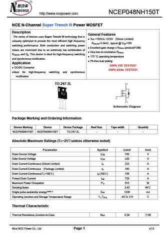
NCEP048NH150T http //www.ncepower.com NCE N-Channel Super Trench III Power MOSFET Description General Features The series of devices uses Super Trench III technology that is V =150V,I =223A (Silicon Limited) DS D uniquely optimized to provide the most efficient high frequency R =3.9m , typical @ V =10V DS(ON) GS switching performance. Both conduction and switching power Ex
9.24. Size:363K ncepower
ncep040n10m.pdf 

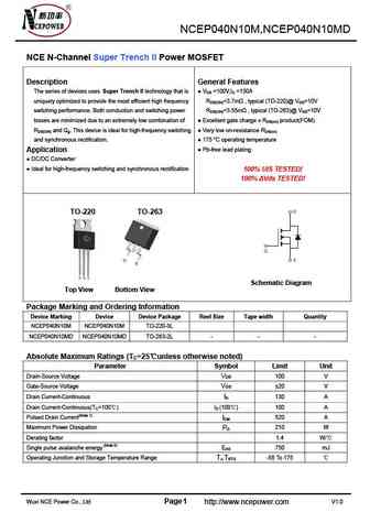
NCEP040N10M,NCEP040N10MD NCE N-Channel Super Trench II Power MOSFET Description General Features The series of devices uses Super Trench II technology that is VDS =100V,ID =130A uniquely optimized to provide the most efficient high frequency RDS(ON)=3.7m , typical (TO-220)@ VGS=10V switching performance. Both conduction and switching power RDS(ON)=3.55m , typical (TO-263)@ VG
9.25. Size:1002K ncepower
ncep040n85m ncep040n85md.pdf 

Pb Free Product NCEP040N85M NCEP040N85MD NCE N-Channel Super Trench II Power MOSFET Description The series of devices uses Super Trench II technology that is General Features uniquely optimized to provide the most efficient high frequency V =85V,I =140A DS D switching performance. Both conduction and switching power R =3.4m , typical (TO-220)@ V =10V DS(ON) GS losses are minimi
9.26. Size:371K ncepower
ncep045n10.pdf 

NCEP045N10,NCEP045N10D NCE N-Channel Super Trench II Power MOSFET Description General Features The series of devices uses Super Trench II technology that is VDS =100V,ID =125A uniquely optimized to provide the most efficient high frequency RDS(ON)=4.2m , typical (TO-220)@ VGS=10V switching performance. Both conduction and switching power RDS(ON)=4.0m , typical (TO-263
9.27. Size:968K ncepower
ncep045n85.pdf 

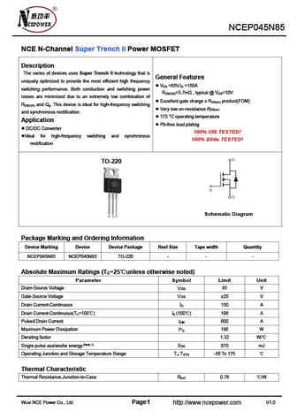
NCEP045N85 NCE N-Channel Super Trench II Power MOSFET Description The series of devices uses Super Trench II technology that is General Features uniquely optimized to provide the most efficient high frequency V =85V,I =150A DS D switching performance. Both conduction and switching power R =3.7m , typical @ V =10V DS(ON) GS losses are minimized due to an extremely low combinatio
9.28. Size:325K ncepower
ncep040n85 ncep040n85d.pdf 

NCEP040N85, NCEP040N85D NCE N-Channel Super Trench II Power MOSFET Description The series of devices uses Super Trench II technology that is General Features uniquely optimized to provide the most efficient high frequency VDS =85V,ID =140A switching performance. Both conduction and switching power RDS(ON)=3.5m , typical (TO-220)@ VGS=10V losses are minimized due to an ext
9.29. Size:371K ncepower
ncep045n10m.pdf 

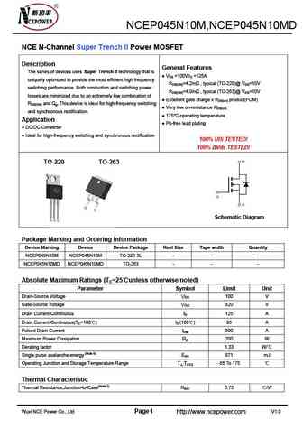
NCEP045N10M,NCEP045N10MD NCE N-Channel Super Trench II Power MOSFET Description General Features The series of devices uses Super Trench II technology that is VDS =100V,ID =125A uniquely optimized to provide the most efficient high frequency RDS(ON)=4.2m , typical (TO-220)@ VGS=10V switching performance. Both conduction and switching power RDS(ON)=4.0m , typical (TO-2
9.30. Size:699K ncepower
ncep040n85d.pdf 

NCEP040N85, NCEP040N85D NCE N-Channel Super Trench II Power MOSFET Description The series of devices uses Super Trench II technology that is General Features uniquely optimized to provide the most efficient high frequency V =85V,I =140A DS D switching performance. Both conduction and switching power R =3.5m , typical (TO-220)@ V =10V DS(ON) GS losses are minimized due to an extr
9.31. Size:706K ncepower
ncep045n85g.pdf 

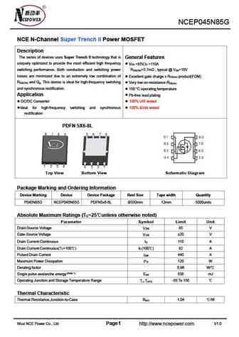
NCEP045N85G NCE N-Channel Super Trench II Power MOSFET Description The series of devices uses Super Trench II technology that is General Features uniquely optimized to provide the most efficient high frequency V =85V,I =110A DS D switching performance. Both conduction and switching power R =3.7m , typical @ V =10V DS(ON) GS losses are minimized due to an extremely low combinatio
9.32. Size:316K ncepower
ncep045n10f.pdf 

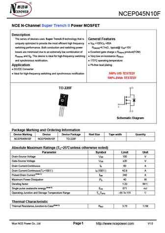
NCEP045N10F NCE N-Channel Super Trench II Power MOSFET Description The series of devices uses Super Trench II technology that is General Features uniquely optimized to provide the most efficient high frequency VDS =100V,ID =60A switching performance. Both conduction and switching power RDS(ON)=4.7m , typical@ VGS=10V losses are minimized due to an extremely low combination o
9.33. Size:985K ncepower
ncep040n10gu.pdf 

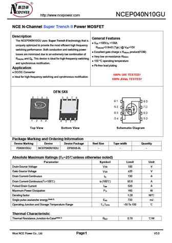
http //www.ncepower.com NCEP040N10GU NCE N-Channel Super Trench II Power MOSFET Description General Features The NCEP040N10GU uses Super Trench II technology that is V =100V,I =130A DS D uniquely optimized to provide the most efficient high frequency R =3.6m (Typ.) @ V =10V DS(ON) GS switching performance. Both conduction and switching power Excellent gate charge x R produc
9.34. Size:835K ncepower
ncep048n85d.pdf 

NCEP048N85M, NCEP048N85MD NCE N-Channel Super Trench II Power MOSFET Description The series of devices uses Super Trench II technology that is General Features uniquely optimized to provide the most efficient high frequency V =85V,I =120A DS D switching performance. Both conduction and switching power R =4.45m , typical (TO-220)@ V =10V DS(ON) GS losses are minimized due to an e
9.35. Size:363K ncepower
ncep040n10 ncep040n10d.pdf 

NCEP040N10,NCEP040N10D NCE N-Channel Super Trench II Power MOSFET Description General Features The series of devices uses Super Trench II technology that is VDS =100V,ID =130A uniquely optimized to provide the most efficient high frequency RDS(ON)=3.7m , typical (TO-220)@ VGS=10V switching performance. Both conduction and switching power RDS(ON)=3.55m , typical (TO-263)@ VGS=
9.36. Size:797K ncepower
ncep048nh150.pdf 

http //www.ncepower.com NCEP048NH150 NCE N-Channel Super Trench III Power MOSFET Description General Features The series of devices uses Super Trench III technology that is V =150V,I =175A DS D uniquely optimized to provide the most efficient high frequency R =3.9m , typical @ V =10V DS(ON) GS switching performance. Both conduction and switching power Excellent gate charge
9.37. Size:400K ncepower
ncep040n12 ncep040n12d.pdf 

NCEP040N12, NCEP040N12D NCE N-Channel Super Trench II Power MOSFET Description General Features The series of devices uses Super Trench II technology that is VDS =120V,ID =150A uniquely optimized to provide the most efficient high frequency RDS(ON)=3.5m , typical (TO-220)@ VGS=10V switching performance. Both conduction and switching power RDS(ON)=3.3m , typical (TO-2
Другие IGBT... CEP01N6G, CEP02N65A, CEP02N65G, CEP02N6A, CEP02N6G, CEP02N7G, CEP02N9, CEP03N8, SPP20N60C3, CEP04N65, CEP04N7G, CEP05N65, CEP06N7, CEP07N65, CEP07N65A, CEP07N7, CEB13N5A
