CES2362. Аналоги и основные параметры
Наименование производителя: CES2362
Тип транзистора: MOSFET
Полярность: N
Предельные значения
Pd ⓘ
- Максимальная рассеиваемая мощность: 1.3 W
|Vds|ⓘ - Максимально допустимое напряжение сток-исток: 60 V
|Vgs|ⓘ - Максимально допустимое напряжение затвор-исток: 20 V
|Id| ⓘ - Максимально допустимый постоянный ток стока: 3 A
Tj ⓘ - Максимальная температура канала: 150 °C
Электрические характеристики
tr ⓘ -
Время нарастания: 3 ns
Cossⓘ - Выходная емкость: 70 pf
RDSonⓘ - Сопротивление сток-исток открытого транзистора: 0.08 Ohm
Тип корпуса: SOT23
Аналог (замена) для CES2362
- подборⓘ MOSFET транзистора по параметрам
CES2362 даташит
..1. Size:423K cet
ces2362.pdf 

CES2362 N-Channel Enhancement Mode Field Effect Transistor FEATURES 60V, 3A, RDS(ON) = 80m @VGS = 10V. RDS(ON) = 100m @VGS = 4.5V. High dense cell design for extremely low RDS(ON). Rugged and reliable. D Lead free product is acquired. SOT-23 package. G D S G S SOT-23 ABSOLUTE MAXIMUM RATINGS TA = 25 C unless otherwise noted Parameter Symbol Limit Units Drain-Source Volta
..2. Size:864K cn vbsemi
ces2362.pdf 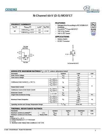
CES2362 www.VBsemi.tw N-Channel 60-V (D-S) MOSFET FEATURES PRODUCT SUMMARY Halogen-free According to IEC 61249-2-21 VDS (V) RDS(on) ( ) ID (A)a Qg (Typ.) Available TrenchFET Power MOSFET 0.085 at VGS = 10 V 4.0 60 2.1 nC 100 % Rg Tested 0.096 at VGS = 4.5 V 3.8 100 % UIS Tested APPLICATIONS Battery Switch DC/DC Converter D TO-236 (SOT23) G 1
9.1. Size:493K cet
ces2307.pdf 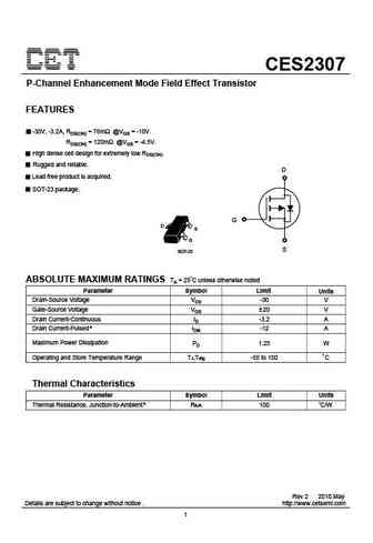
CES2307 P-Channel Enhancement Mode Field Effect Transistor FEATURES -30V, -3.2A, RDS(ON) = 78m @VGS = -10V. RDS(ON) = 120m @VGS = -4.5V. High dense cell design for extremely low RDS(ON). Rugged and reliable. D Lead free product is acquired. SOT-23 package. G D S G S SOT-23 ABSOLUTE MAXIMUM RATINGS TA = 25 C unless otherwise noted Parameter Symbol Limit Units Drain-Sourc
9.2. Size:395K cet
ces2301.pdf 
CES2301 P-Channel Enhancement Mode Field Effect Transistor FEATURES -20V, -2.8A, RDS(ON) = 100m @VGS = -4.5V. RDS(ON) = 150m @VGS = -2.5V. High dense cell design for extremely low RDS(ON). Rugged and reliable. D Lead free product is acquired. SOT-23 package. G D S G S SOT-23 ABSOLUTE MAXIMUM RATINGS TA = 25 C unless otherwise noted Parameter Symbol Limit Units Drain-Sou
9.3. Size:405K cet
ces2302.pdf 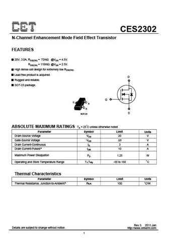
CES2302 N-Channel Enhancement Mode Field Effect Transistor FEATURES 20V, 3.0A, RDS(ON) = 72m @VGS = 4.5V. RDS(ON) = 110m @VGS = 2.5V. High dense cell design for extremely low RDS(ON). Lead free product is acquired. D Rugged and reliable. SOT-23 package. G D S G S SOT-23 ABSOLUTE MAXIMUM RATINGS TA = 25 C unless otherwise noted Parameter Symbol Limit Units Drain-Source V
9.4. Size:635K cet
ces2336.pdf 
CES2336 N-Channel Enhancement Mode Field Effect Transistor PRELIMINARY FEATURES 60V, 1.8A, RDS(ON) = 250m @VGS = 10V. RDS(ON) = 330m @VGS = 4.5V. High dense cell design for extremely low RDS(ON). Rugged and reliable. D Lead free product is acquired. SOT-23 package. G D S G S SOT-23 ABSOLUTE MAXIMUM RATINGS TA = 25 C unless otherwise noted Parameter Symbol Limit Units Dra
9.5. Size:132K cet
ces2303.pdf 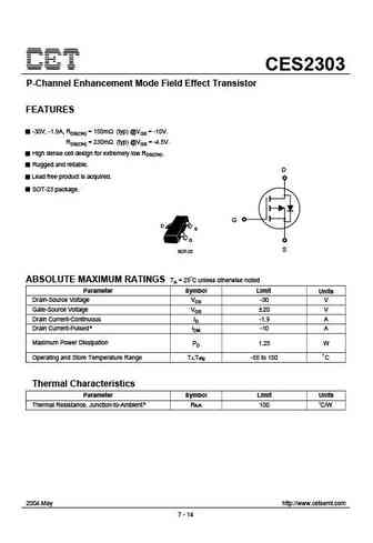
CES2303 P-Channel Enhancement Mode Field Effect Transistor FEATURES -30V, -1.9A, RDS(ON) = 150m (typ) @VGS = -10V. RDS(ON) = 230m (typ) @VGS = -4.5V. High dense cell design for extremely low RDS(ON). Rugged and reliable. D Lead free product is acquired. SOT-23 package. G D S G S SOT-23 ABSOLUTE MAXIMUM RATINGS TA = 25 C unless otherwise noted Parameter Symbol Limit Units
9.6. Size:361K cet
ces2342.pdf 
CES2342 N-Channel Enhancement Mode Field Effect Transistor FEATURES 40V, 4.6A, RDS(ON) = 37m @VGS = 10V. RDS(ON) = 50m @VGS = 4.5V. High dense cell design for extremely low RDS(ON). Rugged and reliable. D Lead-free plating ; RoHS compliant. SOT-23 package. G D S G S SOT-23 ABSOLUTE MAXIMUM RATINGS TA = 25 C unless otherwise noted Parameter Symbol Limit Units Drain-Sourc
9.7. Size:156K cet
ces2308.pdf 
CES2308 N-Channel Enhancement Mode Field Effect Transistor PRELIMINARY FEATURES 20V, 5.4A, RDS(ON) = 27m @VGS = 4.5V. RDS(ON) = 36m @VGS = 2.5V. High dense cell design for extremely low RDS(ON). Rugged and reliable. D Lead free product is acquired. SOT-23 package. G D S G S SOT-23 ABSOLUTE MAXIMUM RATINGS TA = 25 C unless otherwise noted Parameter Symbol Limit Units Drai
9.8. Size:919K cet
ces2322.pdf 
CES2322 N-Channel Enhancement Mode Field Effect Transistor PRELIMINARY FEATURES 20V, 6.2A, RDS(ON) = 22m @VGS = 4.5V. RDS(ON) = 30m @VGS = 2.5V. High dense cell design for extremely low RDS(ON). Lead-free plating ; RoHS compliant. D Rugged and reliable. SOT-23 package. G D S G S SOT-23 ABSOLUTE MAXIMUM RATINGS TA = 25 C unless otherwise noted Parameter Symbol Limit Units
9.9. Size:560K cet
ces2306.pdf 
CES2306 N-Channel Enhancement Mode Field Effect Transistor FEATURES 20V, 3.6A, RDS(ON) = 60m @VGS = 4.5V. RDS(ON) = 70m @VGS = 2.5V. RDS(ON) = 100m @VGS = 1.8V. High dense cell design for extremely low RDS(ON). D Lead free product is acquired. Rugged and reliable. SOT-23 package. G D S G S SOT-23 ABSOLUTE MAXIMUM RATINGS TA = 25 C unless otherwise noted Parameter Sy
9.10. Size:387K cet
ces2323.pdf 
CES2323 P-Channel Enhancement Mode Field Effect Transistor FEATURES -30V, -4.2A, RDS(ON) = 48m @VGS = -10V. RDS(ON) = 80m @VGS = -4.5V. High dense cell design for extremely low RDS(ON). Rugged and reliable. D Lead free product is acquired. SOT-23 package. G D S G S SOT-23 ABSOLUTE MAXIMUM RATINGS TA = 25 C unless otherwise noted Parameter Symbol Limit Units Drain-Source
9.11. Size:390K cet
ces2317.pdf 
CES2317 P-Channel Enhancement Mode Field Effect Transistor FEATURES -30V, -3.1A, RDS(ON) = 80m @VGS = -10V. RDS(ON) = 90m @VGS = -4.5V. RDS(ON) = 120m @VGS = -2.5V. High dense cell design for extremely low RDS(ON). D Rugged and reliable. Lead-free plating ; RoHS compliant. SOT-23 package. G D S G S SOT-23 ABSOLUTE MAXIMUM RATINGS TA = 25 C unless otherwise noted Par
9.12. Size:156K cet
ces2308(esd).pdf _0001.jpg)
CES2308 N-Channel Enhancement Mode Field Effect Transistor PRELIMINARY FEATURES 20V, 5.4A, RDS(ON) = 27m @VGS = 4.5V. RDS(ON) = 36m @VGS = 2.5V. High dense cell design for extremely low RDS(ON). Rugged and reliable. D Lead free product is acquired. SOT-23 package. G D S G S SOT-23 ABSOLUTE MAXIMUM RATINGS TA = 25 C unless otherwise noted Parameter Symbol Limit Units Drai
9.13. Size:141K cet
ces2316.pdf 
CES2316 N-Channel Enhancement Mode Field Effect Transistor FEATURES 30V, 4.8A, RDS(ON) = 34m @VGS = 10V. RDS(ON) = 50m @VGS = 4.5V. High dense cell design for extremely low RDS(ON). Lead free product is acquired. D Rugged and reliable. SOT-23 package. G D S G S SOT-23 ABSOLUTE MAXIMUM RATINGS TA = 25 C unless otherwise noted Parameter Symbol Limit Units Drain-Source Vol
9.14. Size:424K cet
ces2307a.pdf 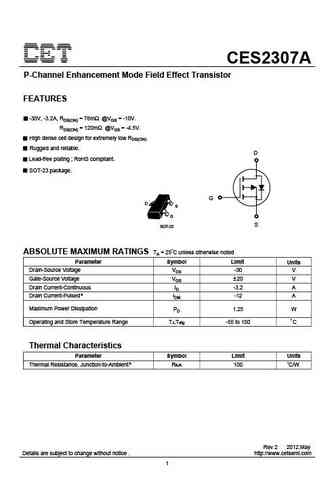
CES2307A P-Channel Enhancement Mode Field Effect Transistor FEATURES -30V, -3.2A, RDS(ON) = 78m @VGS = -10V. RDS(ON) = 120m @VGS = -4.5V. High dense cell design for extremely low RDS(ON). Rugged and reliable. D Lead-free plating ; RoHS compliant. SOT-23 package. G D S G S SOT-23 ABSOLUTE MAXIMUM RATINGS TA = 25 C unless otherwise noted Parameter Symbol Limit Units Drain
9.15. Size:1084K cet
ces2310.pdf 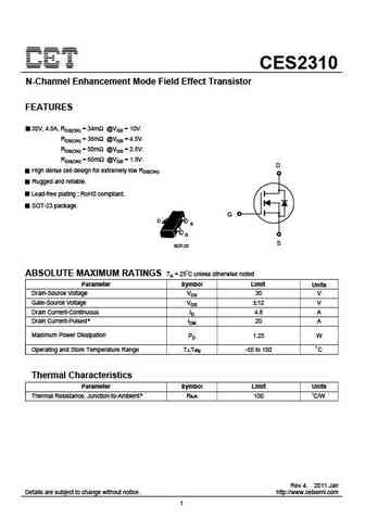
CES2310 N-Channel Enhancement Mode Field Effect Transistor FEATURES 30V, 4.8A, RDS(ON) = 34m @VGS = 10V. RDS(ON) = 38m @VGS = 4.5V. RDS(ON) = 50m @VGS = 2.5V. RDS(ON) = 60m @VGS = 1.8V. D High dense cell design for extremely low RDS(ON). Rugged and reliable. Lead-free plating ; RoHS compliant. SOT-23 package. G D S G S SOT-23 ABSOLUTE MAXIMUM RATINGS TA = 25 C u
9.16. Size:275K cet
ces2312.pdf 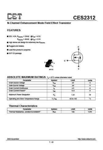
CES2312 N-Channel Enhancement Mode Field Effect Transistor FEATURES 20V, 4.5A, RDS(ON) = 33m @VGS = 4.5V. RDS(ON) = 40m @VGS = 2.5V. High dense cell design for extremely low RDS(ON). Rugged and reliable. D Lead free product is acquired. SOT-23 package. G D S G S SOT-23 ABSOLUTE MAXIMUM RATINGS TA = 25 C unless otherwise noted Parameter Symbol Limit Units Drain-Source Vo
9.17. Size:597K cet
ces2313.pdf 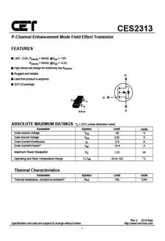
CES2313 P-Channel Enhancement Mode Field Effect Transistor FEATURES -30V, -3.6A, RDS(ON) = 60m @VGS = -10V. RDS(ON) = 90m @VGS = -4.5V. High dense cell design for extremely low RDS(ON). Rugged and reliable. D Lead free product is acquired. SOT-23 package. G D S G S SOT-23 ABSOLUTE MAXIMUM RATINGS TA = 25 C unless otherwise noted Parameter Symbol Limit Units Drain-Source
9.18. Size:389K cet
ces2331.pdf 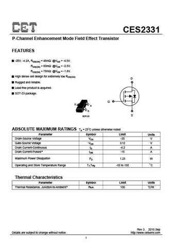
CES2331 P-Channel Enhancement Mode Field Effect Transistor FEATURES -20V, -4.2A, RDS(ON) = 48m @VGS = -4.5V. RDS(ON) = 60m @VGS = -2.5V. RDS(ON) = 78m @VGS = -1.8V. High dense cell design for extremely low RDS(ON). D Rugged and reliable. Lead free product is acquired. SOT-23 package. G D S G S SOT-23 ABSOLUTE MAXIMUM RATINGS TA = 25 C unless otherwise noted Paramete
9.19. Size:139K cet
ces2314.pdf 
CES2314 N-Channel Enhancement Mode Field Effect Transistor FEATURES 30V, 4A, RDS(ON) = 50m @VGS = 10V. RDS(ON) = 70m @VGS = 4.5V. High dense cell design for extremely low RDS(ON). Lead free product is acquired. D Rugged and reliable. SOT-23 package. G D S G S SOT-23 ABSOLUTE MAXIMUM RATINGS TA = 25 C unless otherwise noted Parameter Symbol Limit Units Drain-Source Volta
9.20. Size:453K cet
ces2324.pdf 
CES2324 N-Channel Enhancement Mode Field Effect Transistor FEATURES 20V, 4.2A, RDS(ON) = 45m @VGS = 4.5V. RDS(ON) = 80m @VGS = 2.5V. High dense cell design for extremely low RDS(ON). Lead free product is acquired. D Rugged and reliable. SOT-23 package. G D S G S SOT-23 ABSOLUTE MAXIMUM RATINGS TA = 25 C unless otherwise noted Parameter Symbol Limit Units Drain-Source Vo
9.21. Size:265K cet
ces2305.pdf 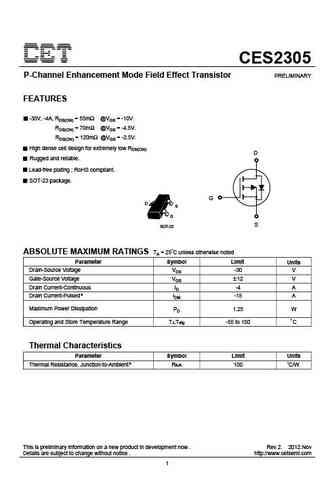
CES2305 P-Channel Enhancement Mode Field Effect Transistor PRELIMINARY FEATURES -30V, -4A, RDS(ON) = 55m @VGS = -10V. RDS(ON) = 70m @VGS = -4.5V. RDS(ON) = 120m @VGS = -2.5V. High dense cell design for extremely low RDS(ON). D Rugged and reliable. Lead-free plating ; RoHS compliant. SOT-23 package. G D S G S SOT-23 ABSOLUTE MAXIMUM RATINGS TA = 25 C unless otherwise
9.22. Size:409K cet
ces2313a.pdf 
CES2313A P-Channel Enhancement Mode Field Effect Transistor FEATURES -30V, -3.8A, RDS(ON) = 55m @VGS = -10V. RDS(ON) = 86m @VGS = -4.5V. High dense cell design for extremely low RDS(ON). Rugged and reliable. D Lead free product is acquired. SOT-23 package. G D S G S SOT-23 ABSOLUTE MAXIMUM RATINGS TA = 25 C unless otherwise noted Parameter Symbol Limit Units Drain-Sourc
9.23. Size:133K cet
ces2309.pdf 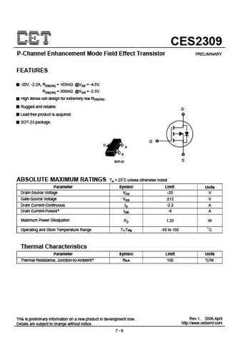
CES2309 P-Channel Enhancement Mode Field Effect Transistor PRELIMINARY FEATURES -20V, -2.2A, RDS(ON) = 165m @VGS = -4.5V. RDS(ON) = 300m @VGS = -2.5V. High dense cell design for extremely low RDS(ON). Rugged and reliable. D Lead free product is acquired. SOT-23 package. G D S G S SOT-23 ABSOLUTE MAXIMUM RATINGS TA = 25 C unless otherwise noted Parameter Symbol Limit Unit
9.24. Size:365K cet
ces2321a.pdf 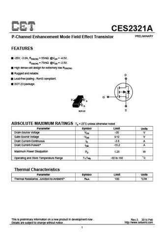
CES2321A PRELIMINARY P-Channel Enhancement Mode Field Effect Transistor FEATURES -20V, -3.8A, RDS(ON) = 55m @VGS = -4.5V. RDS(ON) = 75m @VGS = -2.5V. High dense cell design for extremely low RDS(ON). Rugged and reliable. D Lead-free plating ; RoHS compliant. SOT-23 package. G D S G S SOT-23 ABSOLUTE MAXIMUM RATINGS TA = 25 C unless otherwise noted Parameter Symbol Limit
9.25. Size:378K cet
ces2321.pdf 
CES2321 P-Channel Enhancement Mode Field Effect Transistor FEATURES -20V, -3.8A, RDS(ON) = 55m @VGS = -4.5V. RDS(ON) = 62m @VGS = -2.5V. High dense cell design for extremely low RDS(ON). Rugged and reliable. D Lead free product is acquired. SOT-23 package. G D S G S SOT-23 ABSOLUTE MAXIMUM RATINGS TA = 25 C unless otherwise noted Parameter Symbol Limit Units Drain-Sourc
9.26. Size:478K cet
ces2320.pdf 
CES2320 N-Channel Enhancement Mode Field Effect Transistor FEATURES 30V, 5.2A, RDS(ON) = 29m @VGS = 10V. RDS(ON) = 45m @VGS = 4.5V. High dense cell design for extremely low RDS(ON). Lead free product is acquired. D Rugged and reliable. SOT-23 package. G D S G S SOT-23 ABSOLUTE MAXIMUM RATINGS TA = 25 C unless otherwise noted Parameter Symbol Limit Units Drain-Source Vol
9.27. Size:870K cn vbsemi
ces2307.pdf 
CES2307 www.VBsemi.tw P-Channel 30 V (D-S) MOSFET FEATURES PRODUCT SUMMARY TrenchFET Power MOSFET 100 % Rg Tested VDS (V) RDS(on) ( ) Typ. ID (A)a Qg (Typ.) 0.046 at VGS = - 10 V - 5.6 0.049 at VGS = - 6 V - 5 11.4 nC - 30 APPLICATIONS 0.054 at VGS = - 4.5 V -4.5 For Mobile Computing - Load Switch - Notebook Adaptor Switch S TO-236 - DC/DC Converter (SOT-23)
9.28. Size:870K cn vbsemi
ces2301.pdf 
CES2301 www.VBsemi.tw P-Channel 20-V (D-S) MOSFET FEATURES MOSFET PRODUCT SUMMARY Halogen-free According to IEC 61249-2-21 VDS (V) RDS(on) ( )ID (A)a Qg (Typ.) Definition 0.035 at VGS = - 10 V - 5e TrenchFET Power MOSFET e - 20 0.043 at VGS = - 4.5 V - 5 10 nC 100 % Rg Tested 0.061 at VGS = - 2.5 V - 4.8 Compliant to RoHS Directive 2002/95/EC APPLICATIONS
9.29. Size:1706K cn vbsemi
ces2302.pdf 
CES2302 www.VBsemi.tw N-Channel 20 V (D-S) MOSFET FEATURES PRODUCT SUMMARY Halogen-free According to IEC 61249-2-21 VDS (V) RDS(on) ( ) ID (A)e Qg (Typ.) Definition 0.028 at VGS = 4.5 V TrenchFET Power MOSFET 6a 100 % Rg Tested 20 0.042 at VGS = 2.5 V 6a 8.8 nC Compliant to RoHS Directive 2002/95/EC 0.050 at VGS = 1.8 V 5.6 APPLICATIONS DC/DC C
9.30. Size:869K cn vbsemi
ces2331.pdf 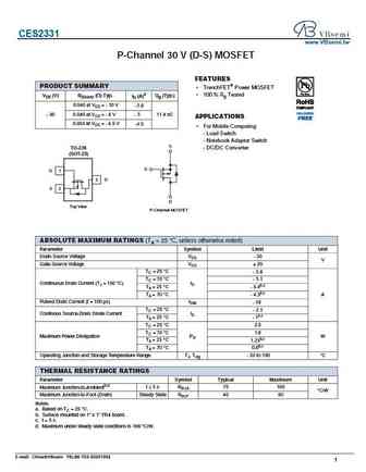
CES2331 www.VBsemi.tw P-Channel 30 V (D-S) MOSFET FEATURES PRODUCT SUMMARY TrenchFET Power MOSFET 100 % Rg Tested VDS (V) RDS(on) ( ) Typ. ID (A)a Qg (Typ.) 0.046 at VGS = - 10 V - 5.6 0.049 at VGS = - 6 V - 5 11.4 nC - 30 APPLICATIONS 0.054 at VGS = - 4.5 V -4.5 For Mobile Computing - Load Switch - Notebook Adaptor Switch S TO-236 - DC/DC Converter (SOT-23)
9.31. Size:1675K cn vbsemi
ces2314.pdf 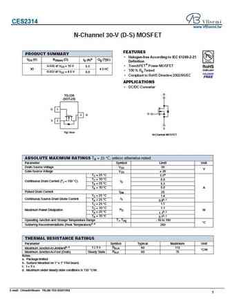
CES2314 www.VBsemi.tw N-Channel 30-V (D-S) MOSFET FEATURES PRODUCT SUMMARY Halogen-free According to IEC 61249-2-21 VDS (V) RDS(on) ( ) ID (A)a Qg (Typ.) Definition 0.030 at VGS = 10 V TrenchFET Power MOSFET 6.5 30 4.5 nC 100 % Rg Tested 0.033 at VGS = 4.5 V 6.0 Compliant to RoHS Directive 2002/95/EC APPLICATIONS DC/DC Converter D TO-236 (SOT-23) G
9.32. Size:1706K cn vbsemi
ces2324.pdf 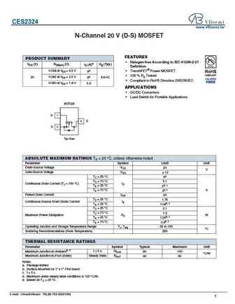
CES2324 www.VBsemi.tw N-Channel 20 V (D-S) MOSFET FEATURES PRODUCT SUMMARY Halogen-free According to IEC 61249-2-21 VDS (V) RDS(on) ( ) ID (A)e Qg (Typ.) Definition 0.028 at VGS = 4.5 V TrenchFET Power MOSFET 6a 100 % Rg Tested 20 0.042 at VGS = 2.5 V 6a 8.8 nC Compliant to RoHS Directive 2002/95/EC 0.050 at VGS = 1.8 V 5.6 APPLICATIONS DC/DC C
9.33. Size:871K cn vbsemi
ces2321.pdf 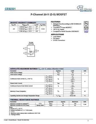
CES2321 www.VBsemi.tw P-Channel 20-V (D-S) MOSFET FEATURES MOSFET PRODUCT SUMMARY Halogen-free According to IEC 61249-2-21 VDS (V) RDS(on) ( )ID (A)a Qg (Typ.) Definition 0.035 at VGS = - 10 V - 5e TrenchFET Power MOSFET e - 20 0.043 at VGS = - 4.5 V - 5 10 nC 100 % Rg Tested 0.061 at VGS = - 2.5 V - 4.8 Compliant to RoHS Directive 2002/95/EC APPLICATIONS
Другие IGBT... CES2308, CES2310, CES2312, CES2314, CES2316, CES2320, CES2324, CES2342, IRF640N, CET0215, CET04N10, CET3055L, CET3252, CET6426, CEU4269, CEU4279, CEV2306
