FDV303N. Аналоги и основные параметры
Наименование производителя: FDV303N
Тип транзистора: MOSFET
Полярность: N
Предельные значения
Pd ⓘ
- Максимальная рассеиваемая мощность: 0.35 W
|Vds|ⓘ - Максимально допустимое напряжение сток-исток: 25 V
|Vgs|ⓘ - Максимально допустимое напряжение затвор-исток: 8 V
|Id| ⓘ - Максимально допустимый постоянный ток стока: 0.68 A
Tj ⓘ - Максимальная температура канала: 150 °C
Электрические характеристики
RDSonⓘ - Сопротивление сток-исток открытого транзистора: 0.45 Ohm
Тип корпуса: SOT23
Аналог (замена) для FDV303N
- подборⓘ MOSFET транзистора по параметрам
FDV303N даташит
..1. Size:47K fairchild semi
fdv303n nb9u008.pdf 

August 1997 FDV303N Digital FET, N-Channel General Description Features 25 V, 0.68 A continuous, 2 A Peak. These N-Channel enhancement mode field effect transistors are RDS(ON) = 0.45 @ VGS = 4.5 V produced using Fairchild's proprietary, high cell density, DMOS technology. This very high density process is tailored to minimize RDS(ON) = 0.6 @ VGS= 2.7 V. on-state resistanc
..2. Size:65K fairchild semi
fdv303n.pdf 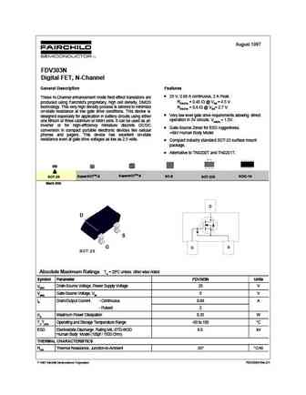
August 1997 FDV303N Digital FET, N-Channel General Description Features 25 V, 0.68 A continuous, 2 A Peak. These N-Channel enhancement mode field effect transistors are RDS(ON) = 0.45 @ VGS = 4.5 V produced using Fairchild's proprietary, high cell density, DMOS technology. This very high density process is tailored to minimize RDS(ON) = 0.6 @ VGS= 2.7 V. on-state resistanc
..3. Size:1238K kexin
fdv303n.pdf 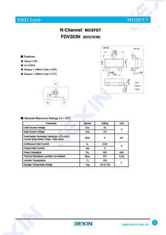
SMD Type MOSFET N-Channel MOSFET FDV303N (KDV303N) SOT-23 Unit mm +0.1 2.9 -0.1 +0.1 0.4 -0.1 3 Features VDS (V) = 25V ID = 0.68 A 1 2 RDS(ON) 450m (VGS = 4.5V) +0.1 +0.05 0.95-0.1 0.1-0.01 +0.1 RDS(ON) 600m (VGS = 2.7V) 1.9-0.1 1.Gate D 2.Source 3.Drain G S Absolute Maximum Ratings Ta = 25 Parameter Symbol Rating Unit Dra
..4. Size:546K cn shikues
fdv303n.pdf 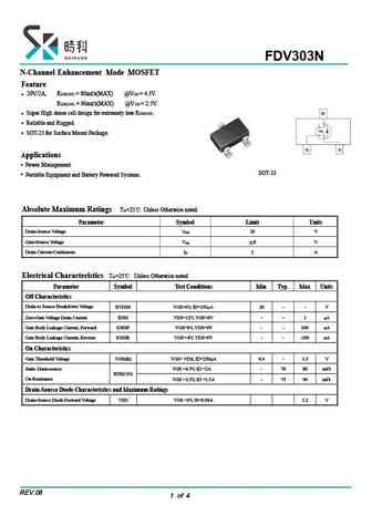
FDV303N N-Channel Enhancement Mode MOSFET Feature 20V/2A, RDS(ON) = 80m (MAX) @VGS = 4.5V. RDS(ON) = 90m (MAX) @VGS = 2.5V. Super High dense cell design for extremely low RDS(ON) . Reliable and Rugged. SOT-23 for Surface Mount Package. Applications Power Management SOT-23 Portable Equipment and Battery Powered Systems. Absolute Maximum Ratings TA=
..5. Size:2319K cn vbsemi
fdv303n.pdf 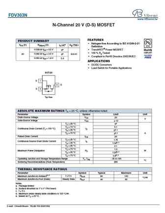
FDV303N www.VBsemi.tw N-Channel 20 V (D-S) MOSFET FEATURES PRODUCT SUMMARY Halogen-free According to IEC 61249-2-21 VDS (V) RDS(on) ( ) ID (A)e Qg (Typ.) Definition 0.028 at VGS = 4.5 V TrenchFET Power MOSFET 6a 100 % Rg Tested 20 0.042 at VGS = 2.5 V 6a 8.8 nC Compliant to RoHS Directive 2002/95/EC 0.050 at VGS = 1.8 V 5.6 APPLICATIONS DC/DC C
0.1. Size:1245K kexin
fdv303n-3.pdf 
SMD Type MOSFET N-Channel MOSFET FDV303N (KDV303N) SOT-23-3 Unit mm +0.2 2.9-0.1 +0.1 0.4 -0.1 3 Features VDS (V) = 25V ID = 0.68 A 1 2 RDS(ON) 450m (VGS = 4.5V) +0.02 +0.1 0.15 -0.02 0.95 -0.1 +0.1 1.9-0.2 RDS(ON) 600m (VGS = 2.7V) 1.Gate D 2.Source 3.Drain G S Absolute Maximum Ratings Ta = 25 Parameter Symbol Rating Unit
9.1. Size:173K fairchild semi
fdv301n d87z fdv301n nb9v005.pdf 
June 2009 FDV301N Digital FET , N-Channel General Description Features 25 V, 0.22 A continuous, 0.5 A Peak. This N-Channel logic level enhancement mode field effect RDS(ON) = 5 @ VGS= 2.7 V transistor is produced using Fairchild's proprietary, high cell density, DMOS technology. This very high density process is RDS(ON) = 4 @ VGS= 4.5 V. especially tailored to minimize on-
9.2. Size:172K fairchild semi
fdv305n.pdf 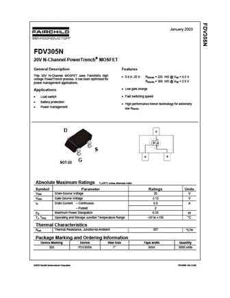
January 2003 FDV305N 20V N-Channel PowerTrench MOSFET General Description Features This 20V N-Channel MOSFET uses Fairchild s high 0.9 A, 20 V RDS(ON) = 220 m @ VGS = 4.5 V voltage PowerTrench process. It has been optimized for RDS(ON) = 300 m @ VGS = 2.5 V power management applications. Low gate charge Applications Fast switching speed Load s
9.3. Size:63K fairchild semi
fdv302p.pdf 
October 1997 FDV302P Digital FET, P-Channel General Description Features -25 V, -0.12 A continuous, -0.5 A Peak. This P-Channel logic level enhancement mode field effect RDS(ON) = 13 @ VGS= -2.7 V transistor is produced using Fairchild's proprietary, high cell density, DMOS technology. This very high density process is RDS(ON) = 10 @ VGS = -4.5 V. especially tailored t
9.4. Size:46K fairchild semi
fdv302p d87z fdv302p nb8v001.pdf 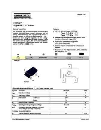
October 1997 FDV302P Digital FET, P-Channel General Description Features -25 V, -0.12 A continuous, -0.5 A Peak. This P-Channel logic level enhancement mode field effect RDS(ON) = 13 @ VGS= -2.7 V transistor is produced using Fairchild's proprietary, high cell density, DMOS technology. This very high density process is RDS(ON) = 10 @ VGS = -4.5 V. especially tailored t
9.5. Size:46K fairchild semi
fdv304p d87z fdv304p nb8u003.pdf 
August 1997 FDV304P Digital FET, P-Channel General Description Features -25 V, -0.46 A continuous, -1.5 A Peak. This P-Channel enhancement mode field effect transistors is produced using Fairchild's proprietary, high cell density, DMOS RDS(ON) = 1.1 @ VGS = -4.5 V technology. This very high density process is tailored to minimize RDS(ON) = 1.5 @ VGS= -2.7 V. on-state resi
9.6. Size:213K fairchild semi
fdv301n.pdf 
June 2009 FDV301N Digital FET , N-Channel General Description Features 25 V, 0.22 A continuous, 0.5 A Peak. This N-Channel logic level enhancement mode field effect RDS(ON) = 5 @ VGS= 2.7 V transistor is produced using Fairchild's proprietary, high cell density, DMOS technology. This very high density process is RDS(ON) = 4 @ VGS= 4.5 V. especially tailored to minimize on-
9.7. Size:63K fairchild semi
fdv304p.pdf 
August 1997 FDV304P Digital FET, P-Channel General Description Features -25 V, -0.46 A continuous, -1.5 A Peak. This P-Channel enhancement mode field effect transistors is produced using Fairchild's proprietary, high cell density, DMOS RDS(ON) = 1.1 @ VGS = -4.5 V technology. This very high density process is tailored to minimize RDS(ON) = 1.5 @ VGS= -2.7 V. on-state resi
9.8. Size:289K onsemi
fdv305n.pdf 
Is Now Part of To learn more about ON Semiconductor, please visit our website at www.onsemi.com Please note As part of the Fairchild Semiconductor integration, some of the Fairchild orderable part numbers will need to change in order to meet ON Semiconductor s system requirements. Since the ON Semiconductor product management systems do not have the ability to manage part nomenclatur
9.9. Size:165K onsemi
fdv302p.pdf 
Is Now Part of To learn more about ON Semiconductor, please visit our website at www.onsemi.com ON Semiconductor and the ON Semiconductor logo are trademarks of Semiconductor Components Industries, LLC dba ON Semiconductor or its subsidiaries in the United States and/or other countries. ON Semiconductor owns the rights to a number of patents, trademarks, copyrights, trade secrets, and oth
9.10. Size:213K onsemi
fdv301n.pdf 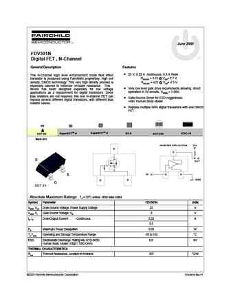
June 2009 FDV301N Digital FET , N-Channel General Description Features 25 V, 0.22 A continuous, 0.5 A Peak. This N-Channel logic level enhancement mode field effect RDS(ON) = 5 @ VGS= 2.7 V transistor is produced using Fairchild's proprietary, high cell density, DMOS technology. This very high density process is RDS(ON) = 4 @ VGS= 4.5 V. especially tailored to minimize on-
9.11. Size:67K onsemi
fdv304p.pdf 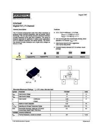
August 1997 FDV304P Digital FET, P-Channel General Description Features -25 V, -0.46 A continuous, -1.5 A Peak. This P-Channel enhancement mode field effect transistors is produced using Fairchild's proprietary, high cell density, DMOS RDS(ON) = 1.1 @ VGS = -4.5 V technology. This very high density process is tailored to minimize RDS(ON) = 1.5 @ VGS= -2.7 V. on-state resi
9.12. Size:1797K kexin
fdv301n.pdf 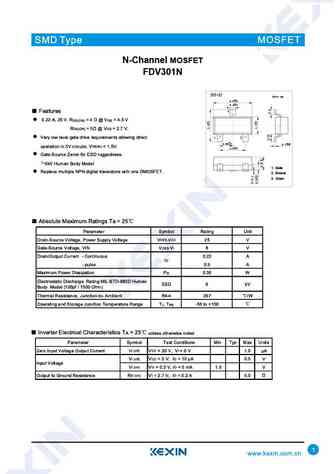
N-Channel MOSFET FDV301N SOT-23 Unit mm +0.1 2.9 -0.1 +0.1 0.4 -0.1 3 1 2 +0.1 +0.05 0.95-0.1 0.1-0.01 +0.1 1.9-0.1 1. Gate 2. Source 3. Drain 0.4 +0.1 +0.1 2.4 -0.1 1.3 -0.1 0.55 +0.1 0.97 -0.1 +0.1 0-0.1 0.38 -0.1 N-Channel MOSFET FDV301N Marking Marking 301 SMD Type MOSFET N-Channel MOSFET FDV301N Typical Characterisitics 1.4 0.5 V GS = 4
9.13. Size:2795K slkor
fdv301n.pdf 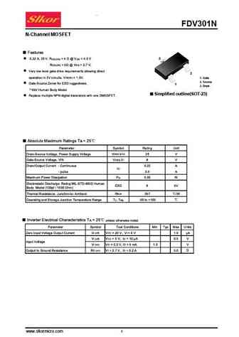
FDV301N N-Channel MOSFET 3 2 1. Gate 2. Source 1 3. Drain Simplified outline(SOT-23) www.slkormicro.com 1 FDV301N www.slkormicro.com 2 FDV301N Typical Characterisitics 1.4 0.5 V GS = 4.5V 4.0 3.5 VG S = 2.0V 0.4 3 .0 1.2 2 .7 2.5 2.5 0.3 2 .7 1 3.0 0.2 2 .0 3 .5 4 .0 0.8 4 .5 0.1 1.5 0 0.6 0 0 .5 1 1.5 2 2.5 3 0 0 .1 0 .2 0 .3 0 .4 0.5 V , DRAIN
9.14. Size:2320K cn vbsemi
fdv301n.pdf 
FDV301N www.VBsemi.tw N-Channel 20 V (D-S) MOSFET FEATURES PRODUCT SUMMARY Halogen-free According to IEC 61249-2-21 VDS (V) RDS(on) ( ) ID (A)e Qg (Typ.) Definition 0.028 at VGS = 4.5 V TrenchFET Power MOSFET 6a 100 % Rg Tested 20 0.042 at VGS = 2.5 V 6a 8.8 nC Compliant to RoHS Directive 2002/95/EC 0.050 at VGS = 1.8 V 5.6 APPLICATIONS DC/DC C
9.15. Size:1509K cn vbsemi
fdv304p.pdf 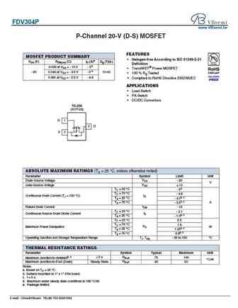
FDV304P www.VBsemi.tw P-Channel 20-V (D-S) MOSFET FEATURES MOSFET PRODUCT SUMMARY Halogen-free According to IEC 61249-2-21 VDS (V) RDS(on) ( )ID (A)a Qg (Typ.) Definition 0.035 at VGS = - 10 V - 5e TrenchFET Power MOSFET e - 20 0.043 at VGS = - 4.5 V - 5 10 nC 100 % Rg Tested 0.061 at VGS = - 2.5 V - 4.8 Compliant to RoHS Directive 2002/95/EC APPLICATIONS
Другие IGBT... FDS9435A, FDS9933A, FDS9936A, FDT439N, FDT457N, FDT459N, FDV301N, FDV302P, 10N65, FDV304P, FK10KM-10, FK10KM-12, FK10KM-9, FK10SM-10, FK10SM-12, FK10SM-9, FK10UM-10
